Am. Chem. Soc.,2014,136 (6), pp 2564–2574.
Florian Le Formal *†, Stephanie R. Pendlebury †,Maurin Cornuz ‡, S. David Tilley ‡, Michael Grätzel ‡, James R. Durrant
*†† Department of Chemistry, Imperial College London, South Kensington Campus, London SW7 2AZ, United Kingdom and
‡ Institut des Sciences et Ingénierie Chimiques, Ecole Polytechnique Fédérale de Lausanne, Laboratory of Photonics and Interfaces, Station 6, CH-1015 Lausanne,Switzerland.
Abstract
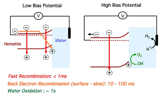
The kinetic competition between electron–hole recombination and water oxidation is a key consideration for the development of efficient photoanodes for solar driven water splitting. In this study, we employed three complementary techniques, transient absorption spectroscopy (TAS), transient photocurrent spectroscopy (TPC), and electrochemical impedance spectroscopy (EIS), to address this issue for one of the most widely studied photoanode systems: nanostructured hematite thin films. For the first time, we show a quantitative agreement between all three techniques. In particular, all three methods show the presence of a recombination process on the 10 ms to 1 s time scale, with the time scale and yield of this loss process being dependent upon applied bias. From comparison of data between these techniques, we are able to assign this recombination phase to recombination of bulk hematite electrons with long-lived holes accumulated at the semiconductor/electrolyte interface. The data from all three techniques are shown to be consistent with a simple kinetic model based on competition between this, bias dependent, recombination pathway and water oxidation by these long-lived holes. Contrary to most existing models, this simple model does not require the consideration of surface states located energetically inside the band gap. These data suggest two distinct roles for the space charge layer developed at the semiconductor/electrolyte interface under anodic bias. Under modest anodic bias (just anodic of flatband), this space charge layer enables the spatial separation of initially generated electrons and holes following photon absorption, generating relatively long-lived holes (milliseconds) at the semiconductor surface. However, under such modest bias conditions, the energetic barrier generated by the space charge layer field is insufficient to prevent the subsequent recombination of these holes with electrons in the semiconductor bulk on a time scale faster than water oxidation. Preventing this back electron–hole recombination requires the application of stronger anodic bias, and is a key reason why the onset potential for photocurrent generation in hematite photoanodes is typically ∼500 mV anodic of flat band and therefore needs to be accounted for in electrode design for PEC water splitting.
Copyright © 2014 American Chemical Society.