Significance
The advancement of photovoltaic (PV) technologies is critical for meeting global energy demands sustainably. Multi-junction solar cells, which incorporate multiple layers of semiconductors with different bandgaps, have the potential to significantly enhance the efficiency of solar energy conversion. An important component of these multi-junction cells is the wide-bandgap top cell, which ideally should possess a bandgap around 2 eV. This requirement has driven extensive research into developing new materials that combine high efficiency, stability, and environmental compatibility. Quaternary copper-silver-bismuth-iodide (Cu-Ag-Bi-I) compounds, particularly Cu2AgBiI6, have emerged as promising candidates due to their intrinsic wide-bandgap (2 eV), direct bandgap nature, and favorable optoelectronic properties. These materials offer potential benefits over traditional lead-based perovskites, including reduced toxicity and better environmental stability. Despite these advantages, several challenges hinder the practical implementation of Cu2AgBiI6 in photovoltaic devices. One of the primary challenges is the complexity of synthesizing high-quality Cu2AgBiI6 thin films with controlled phase purity and optimal morphological characteristics. The material’s multi-element nature makes it prone to phase segregation and the formation of impurities, such as CuI and BiI3, which can adversely affect its electronic and optical properties. Additionally, achieving uniform and defect-free films is crucial for efficient charge-carrier transport and minimizing recombination losses in solar cells. Another significant issue is the charge-carrier dynamics within Cu2AgBiI6. Previous studies have indicated that charge carriers in these materials tend to localize quickly, leading to reduced mobility and increased recombination rates. This behavior is often exacerbated by the presence of impurities and defects, which can act as traps for charge carriers, further diminishing the material’s photovoltaic performance.
Given these challenges, new study published in Advanced Energy Materials and conducted by Dr. Benjamin Putland, Dr. Marcello Righetto, Dr. Heon Jin, Dr. Markus Fischer, Dr. Alexandr Ramadan, Dr. Karl-Augustin Zaininger, Dr. Laura Herz, Dr. Harry Sansom, and led by Professor Henry Snaith from the University of Oxford investigated the effects of processing conditions, specifically annealing temperatures, on the structural, morphological, and optoelectronic properties of vapor-deposited Cu2AgBiI6 thin films. By employing vapor phase co-evaporation, a scalable and controllable deposition technique, the researchers aimed to fabricate high-quality Cu2AgBiI6 films and identify the key factors influencing their performance in photovoltaic applications.
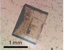
The researchers employed a multi-source co-evaporation technique to fabricate Cu2AgBiI6 thin films, with each precursor (CuI, AgI, and BiI3) evaporated under high vacuum conditions. The goal was to create uniform, approximately 250 nm thick films. The composition of the films was verified using scanning electron microscopy energy dispersive X-ray spectroscopy (SEM-EDX), confirming that the average composition closely matched the nominal target. The SEM-EDX results indicated that the films had an average composition of Cu2.12(12)Ag1.04(18)Bi0.95(7)I6.00(14), demonstrating the success of the co-evaporation process in achieving the desired stoichiometry within acceptable error margins. To understand the phase composition and morphology of the films, the researchers conducted X-ray diffraction (XRD) and scanning electron microscopy (SEM) analyses on both unannealed and annealed samples (at 110 °C, 130 °C, and 150 °C). The XRD patterns revealed a predominantly trigonal phase in unannealed films, with small impurity peaks corresponding to BiI3. Upon annealing, these impurity peaks increased, especially those related to CuI and metallic bismuth, indicating phase transformations and the emergence of additional phases at higher temperatures. They found the annealing process induced significant changes in the films’ morphology. Moreover, SEM images showed that annealed films exhibited larger grain sizes and an increased density of pinholes compared to unannealed films. This morphological degradation at higher temperatures was linked to the presence of CuI and BiI3 impurities, which were more pronounced in the 150 °C annealed samples. They also examined the electronic band structure and optical properties of the films using ultraviolet photoelectron spectroscopy (UPS) and ultraviolet-visible (UV-Vis) absorption spectroscopy. The UPS measurements showed a deepening of the valence band maximum (VBM) with increasing annealing temperature, shifting from -5.2 eV in unannealed films to -5.5 eV in 150 °C annealed films. This shift was attributed to the loss of Cu+ ions from the Cu2AgBiI6 structure, leading to the formation of CuI domains. The UV-Vis absorption spectra revealed strong visible light absorption across all films, with a red shift in the absorption onset as the annealing temperature increased. The bandgap of the unannealed films was calculated to be 2.13 eV, decreasing slightly to approximately 2.10 eV for annealed films. Additionally, an absorption peak at around 415 nm was observed, which became more pronounced with higher annealing temperatures, indicating the presence of CuI-rich impurity phases. The authors used steady-state photoluminescence spectroscopy was used to assess the films’ emission properties. The PL intensity increased with annealing temperature, with a prominent emission peak at 730 nm. This peak was attributed to defect-mediated transitions in CuI, rather than the intrinsic properties of Cu2AgBiI6. Optical pump terahertz probe (OPTP) spectroscopy provided insights into charge-carrier dynamics, revealing that the presence of CuI domains significantly affected the photoconductivity and mobility of the films. The authors’ findings on PL spectroscopy indicated that the enhanced emission in annealed films was due to CuI defect states. The OPTP results showed that charge carriers in Cu2AgBiI6 films quickly localized, reducing mobility and increasing recombination rates. This localization was more pronounced in annealed films, suggesting that CuI impurities acted as charge-carrier traps, hindering efficient charge transport. Moreover, the researchers fabricated planar heterojunction solar cell devices using both unannealed and annealed Cu2AgBiI6 films. These devices were characterized under simulated sunlight to evaluate their photovoltaic performance. The best device, using an unannealed film, achieved a power conversion efficiency (PCE) of 0.43%, with a moderate open-circuit voltage (Voc) and short-circuit current density (Jsc). According to the authors the unannealed film device showed the highest PCE, annealed film devices exhibited more consistent performance across multiple batches. Annealed films generally had higher Voc, Jsc, fill factor (FF), and PCE than unannealed films, despite the increased presence of CuI impurities. External quantum efficiency (EQE) measurements indicated significant photocurrent losses, especially when devices were illuminated from the back side, highlighting poor electron transport as a major limitation.
In conclusion, Professor Henry Snaith and team study has several important implications because it revealed the critical role of CuI impurities in influencing the charge-carrier dynamics and overall performance of Cu2AgBiI6 films. This finding highlights the need to control impurity levels to improve charge transport and reduce recombination losses, which are key factors in enhancing the efficiency of photovoltaic devices. understanding the effects of annealing and impurities on Cu2AgBiI6 films, researchers can develop strategies to minimize defects and optimize film quality. This could lead to more efficient and reliable photovoltaic devices, contributing to the advancement of solar energy technology. Additionally, the use of vapor phase co-evaporation demonstrated in this study is a scalable technique that can be applied in industrial settings. Optimizing this process for Cu2AgBiI6 could facilitate the large-scale production of high-performance solar cells, making them more accessible and cost-effective.


Reference
Benjamin W. J. Putland, Marcello Righetto, Heon Jin, Markus Fischer, Alexandra J. Ramadan, Karl-Augustin Zaininger, Laura M. Herz, Harry C. Sansom, Henry J. Snaith. Compositional Transformation and Impurity-Mediated Optical Transitions in Co-Evaporated Cu2AgBiI6 Thin Films for Photovoltaic Applications. Advanced Energy Materials. Volume 14, Issue 8, February 23, 2024, 2303313