
Significance Statement
Current memory density of magnetic hard drives has increased by using existing 2D device. However, a promising concept, racetrack memory which involves movement of domain walls DW can be utilized to increase the number of layers where bits are stored. Despite the fact that a 3D device is contained in racetrack memory concepts where data bits are stored in tracks perpendicular to a substrate, progress has only been achieved by 2D in-plane thin film geometries.
Researchers led by Professor Jürgen Kosel at King Abdullah University of Science and Technology (KAUST) have now shown that modulated nanowires consisting of alternating nickel Ni and cobalt Co sections facilitate efficient domain wall pinning at interfaces of the sections. The work published in ACS Nano, explained the pinning effect as interaction of stray fields generated at the interface and domain wall using electron holography and micro magnetic simulations.
Magnetic cylindrical nanowires NWs grown in an isolating template perpendicular to a substrate are very promising candidates in realization of 3D magnetic memory devices with a small footprint. They provide high level of control over morphology, geometry, crystal structure and packing density of NWs when fabricated by template-assisted electrodeposition techniques and higher operational speed at faster magnitude than planar devices due to absence of Walker breakdown phenomena.
Low-magnification scanning transmission electron microscopy LM-STEM images were acquired on a Titan 60-300 electron microscope equipped with a high brightness electron gun (x-FEG) and Fischione high angle annual dark field scanning transmission electron microscopy detector.
The TEM was used in Lorentz mode for producing holograms of remanent magnetic states on nanowires. The MAGPAR finite element software package was used to simulate the magnetization process of cobalt, nickel and Co/Ni nanowires.
Pinning and configuration of domain walls was investigated using a combination of magnetic force microscopy MFM, differential phase contrast DPC and electron holography methods. Nanowires were obtained by alternating electrodeposition of cobalt and nickel into aluminum oxide templates.
Results from scanning electron microscopy SEM images showed nanowires embedded inside the aluminum oxide templates had a high uniformity of the length and diameter. X-ray diffraction data revealed high crystallinity with <100> direction and <220> direction for hexagonal close packed hcp cobalt and face center cubic fcc nickel, respectively, close to the growth direction of the nanowires.
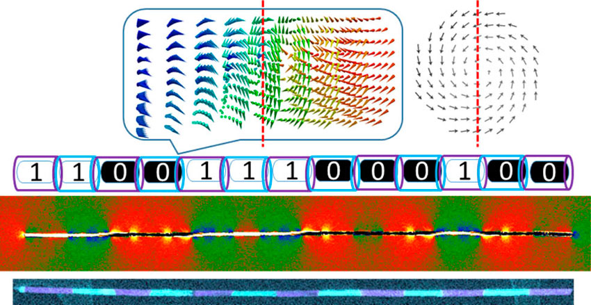
Transmission electron microscopy TEM and electron energy loss spectroscopy EELS confirmed a sharp transition between cobalt and nickel segments. Adopted virtual bright field detector-differential phase contrast VBF-DPC enhanced visualization of the magnetic fields with 4nm resolution and showed the magnetic structure of the nanowires at remanence. They are magnetized in their length-direction with a strong periodic contrast caused by the difference in magnetization value, leading to stray fields outside the cobalt segments in opposite direction to the magnetization.
Electron hologram measurements revealed good agreement with virtual bright field detector-differential phase contrast. Strong stray fields were clearly visible at the interface and outside of the cobalt sections. Spins were pointing along the nanowire in the nickel side where shape anisotropy dominates, while they were forming a complex vortex structure in the cobalt side having a pronounced crystalline anisotropy perpendicular to the nanowire axis.
Field vectors from two measured orthogonal components revealed domain walls located in a distance of about 100-120nm away from interfaces, proving that these interfaces are efficient pinning sites. Micro-magnetic simulation of the 3D vortex domain walls showed excellent agreement with experimental observations.
The results reveal an efficient way to solve a crucial issue related to current driven domain walls motion in cylindrical nanowires, Professor Kosel says, which is promising for high-density data storage devices.


Journal Reference
Yurii P. Ivanov*1, Andrey Chuvilin2,3, Sergei Lopatin1, Jurgen Kosel*1. Modulated Magnetic Nanowires for Controlling Domain Wall Motion: Toward 3D Magnetic Memories. ACS Nano, 2016, 10 (5), pp 5326–5332.
[expand title=”Show Affiliations”]- King Abdullah University of Science and Technology, Thuwal 23955, Saudi Arabia
- CIC nanoGUNE Consolider, Avenida de Tolosa 76, 20018 San Sebastian, Spain
- IKERBASQUE, Basque Foundation for Science, Maria Diaz de Haro 3, 48013 Bilbao,Spain [/expand]
Go To ACS Nano
