
Significance
A Schottky diode is an electronic component that primarily consists of a semiconductor-metal junction. This diode, unlike a normal semiconductor diode, can be turned on and off very quickly. When a 2D material is brought into contact with a bulk material or another 2D material, a 2D-material-based Schottky heterostructure is formed. Formation of such heterostructures is an inevitable process in many optoelectronics and nano-electronics applications. Over the years, 2D-material-based Schottky heterostructures have garnered considerable research attention owing to their wide applicability in various fields. Unfortunately, several discrepancies and misperceptions regarding their carrier transport physics still persist in literature. Although recent works have shed light on the growth, structural, thermal, electrostatic, electronic, and electrical properties of 2D-material-based lateral Schottky heterostructure, a consistent model remains lacking.
In line with this, Dr. Yee Sin Ang , Professor Hui Ying Yang and Professor Lay Kee Ang from the SUTD-MIT International Design Center & Science and Math Cluster at Singapore University of Technology and Design (SUTD) developed generalized analytical reversed saturation current (RSC) models for lateral Schottky heterostructure (LSH) and vertical Schottky heterostructure (VSH) over a wide range of 2D electronic systems, including nonrelativistic electron gas, Rashba spintronic systems, single- and few-layer graphene, and thin films of topological solids. Their model anticipated that the 2D-material-based LSH and VSH are governed by completely different charge transport equations, which can be characterized by a simple universal scaling exponent. Their work is currently published in the research journal, Physical Review Letters.
The research method employed considered a 2D nanosheet in contact with a bulk or 2D semiconductor via its edge to form LSH or via its planar surface to form VSH. Next, a generalized analytical RSC model for LSH and VSH was developed. Finally, the researchers demonstrated that the generalized model is directly applicable for a large variety of 2D electronic systems.
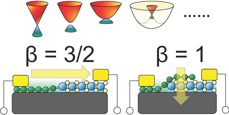
The authors observed that the classic diode scaling of β=2 for a nonrelativistic electrons in bulk material was no longer valid for 2D materials. As a consequence, they developed universal scaling laws which provided a simple useful tool for the analysis of carrier transport and for the extraction of Schottky barrier height in 2D material Schottky heterostructures. Lastly, based on the experimental results of the graphene-based vertical Schottky heterostructure, they noted that the β=1 scaling provided a better fitting with the experimental data as compared to that of the classic β=2 scaling.
In a nutshell, the SUTD study demonstrated the emergence of a universal scaling exponent β=3/2 in LSH, and β=1 in VSH with scattering-induced momentum non-conservation effect. They noted that their model had resolved some of the conflicting results from prior works and was in agreement with recent experiments. Altogether, the findings reported by SUTD scientists have the potential to provide a simple theoretical tool for the description of 2D-material-based heterostructures, thus paving the way for both a fundamental understanding of nanoscale interface physics and applied device engineering.
“The new theory has far reaching impact in solid state physics,” said principal investigator of this research, Prof. Lay Kee Ang, “It signals the breakdown of classic diode equation widely used for traditional materials over the past 60 years, and shall improve our understanding on how to design better 2D material electronics.”


Reference
Yee Sin Ang, Hui Ying Yang, L. K. Ang. Universal Scaling Laws in Schottky Heterostructures Based on Two-Dimensional Materials. Physical Review Letters, volume 121, 056802 (2018)
Go To Physical Review Letters