Significance
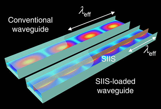
Applications of waveguides in modern technology, such as: in communication and sensing systems, has been largely attributed to their high power-handling capability coupled with low transmission loss. Potential applications include; the high-power microwave and millimeter-wave circuits, radar and satellite communication systems, waveguide-based sensors, and photonic integrated circuits- among others. For waveguides, the cut-off frequency and the dispersion curve are crucial specifications since; for instance, below the cut-off frequency, a waveguide cannot transmit electromagnetic waves, analogous to a high-pass energy conduit. In existing literature, it has been reported that a rectangular waveguide operated slightly above the cut-off frequency can be treated as an effective zero-index medium, because the guided wave exhibits a nearly infinite phase velocity, along with almost uniform and intense electric fields inside the waveguide. Generally, the capability to tailor the dispersion and the cut-off frequency of waveguides is of importance, as these essential parameters govern the operating frequency range and the waveguide dimension.
Recently, Yijing He and Prof. Yue Li at Tsinghua University in collaboration with Liang Zhu, Prof. Danilo Erricolo, and Prof. Pai-Yen Chen at University of Illinois and also Prof. Hakan Bagciat at KAUST proposed a new concept of substrate-integrated impedance surface (SIIS) in a bid to gain arbitrary control of propagation characteristics of closed-shape waveguides. In particular, they focused on developing a theoretical framework for the simplest form of SIIS constituted by a one-dimensional array of blind vias, which is equivalent to a homogenized surface capacitance embedded in the waveguide. Their work is currently published in the research journal, Physical Review Applied.
The scholars derived an explicit formula to describe the surface impedance for the substrate-integrated impedance surface with a specially designed geometry. Next, they calculated the complex propagation constant and dispersion characteristics of a SIIS-loaded waveguide, by solving the transcendental equation. Eventually, to validate the proposed concept, the researchers conducted numerical simulations and experimental characterizations for different on-board SIIS-loaded substrate-integrated waveguides.
The authors observed that the proposed SIIS-loaded SIW could not only ease the implementation complexity, but also enable low propagation loss and high power-carrying capacity. This was seen to be a significant difference when compared with metamaterial-loaded miniature waveguides. Most importantly, validation results obtained from both theoretical and full-wave simulations and experiments were in good agreement, hence validating the model. Remarkably, the large field enhancement in the proximity of the reactive SIIS, as observed, could be used to make ultrasensitive sensors and efficient nonlinear components.
In summary, the study presented the control of waveguide dispersion of an on-aboard or on-chip waveguide by loading a SIIS, constituted by blind/through-hole vias and multilevel interconnect structures. The demonstrated SIIS technique showed great potential for engineering the dispersion and dimensions of versatile waveguide components. Altogether, the presented SIIS-loading technique may open up new possibilities for miniaturization of various waveguide-based components and for enhancement of their uses in sensing and nonlinear functions.


Reference
Yijing He, Yue Li, Liang Zhu, Hakan Bagci, Danilo Erricolo, Pai-Yen Chen. Waveguide Dispersion Tailoring by Using Embedded Impedance Surfaces. Physical Review Applied, volume 10, page 064024 (2018)
Go To Physical Review Applied