
Significance Statement
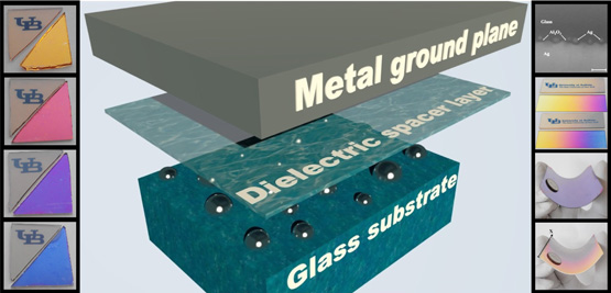
Metasurfaces provide a new planar photonic platform to control the electromagnetic fields in an ultra-thin film with flexibility and performance that was not possible before. A particularly exciting opportunity has emerged in recently developed thin-film metamaterial super absorbers capable of angle- and polarization-insensitive and near-perfect light absorption, which are important optical components required by a variety of applications from photon-harvesting, surface enhanced biosensing and photocatalysis, to thermal energy recycling and near-field heat transfer. However, most reported on-chip optical absorbers usually rely on expensive and small-area top-down micro/nano-lithography. Dr. Qiaoqiang Gan’s group of University at Buffalo, The State University of New York, reported a simple and low-cost method to manufacture scalable super meta-absorbers based on direct sputtering deposition and post-thermal annealing processes which are amenable to continuous roll-to-roll processes for large-area and homogeneous manufacturing. “Using this process”, said Kai Liu, a PhD student in Gan’s group and the first author of this work, “random metallic nanoparticles can easily be formed on both rigid and flexible substrates to function as metasurfaces for large-area metal-dielectric-metal super absorbers. In this case, expensive top-down lithography techniques are unnecessary, and we can fabricate super absorbing metafilms at very large scale.” A unique feature for these super absorbing nanopatterned metal films is that the light is trapped and confined at the nanogap between nanoparticles and realize strongly enhanced localized field. “This localized field enhancement is very promising for the development of novel surface biosensing technologies”, said Xie Zeng, another PhD student in Gan’s team and the leading researcher on biosensor project. This work was collaborated with Dr. Suhua Jiang’s group at Fudan University (Shanghai, China) and was supported by National Science Foundation.
Journal Reference
Nanoscale, 2014,6, 5599-5605.
Kai Liu,a Xie Zeng,a Suhua Jiang,b Dengxin Ji,a Haomin Song,a Nan Zhanga , Qiaoqiang Gan*a .
a-Department of Electrical Engineering, University at Buffalo, The State University of New York, Buffalo, USA
E-mail: [email protected]
b- Department of Materials Science, Fudan University, Shanghai 200433, China.
Abstract
Recently, periodically patterned metasurfaces have been employed to realize on-chip super/near-perfect optical absorption. However, most reported meta-absorbers rely on top-down micro/nano-lithography, which imposed a serious cost barrier for the development of practical applications, especially in visible-infrared domain and at very large scales. We report a simple method to manufacture super absorptive metasurfaces using direct sputtering deposition. By controlling the deposition and post thermal treatment conditions, random metallic nanoparticles (NPs) can be formed easily on rigid and flexible substrates to function as the nanoantennas of spectrally tunable three-layered meta-absorbers. This low-cost and highly scalable approach could overcome the manufacturing cost and area barrier of previously reported meta-absorbers and therefore enable the development of affordable and large-scale thin-film super absorbing metamaterial structures and devices.
© 2014 Royal Society of Chemistry
