Significance Statement
Aluminum amongst different metals offers the most suitable plasmonic material in the ultraviolet range. However, certain structural flaws occur in polycrystalline aluminum nanostructures, which deteriorates their plasmonic performances.
Researchers led by Professor Chih-Kang Shih from University of Texas at Austin developed epitaxially grown aluminum films on silicon as a plasmonic material platform in the ultraviolet range. The research work is now published in peer-reviewed journal ACS Nano.
The authors used a molecular beam epitaxy system to develop an epitaxial growth of single-crystalline aluminum films on silicon substrates. They also used spectroscopic ellipsometry measurements and numerical simulations to ascertain the enhanced optical performance of the single-crystalline Al film and a plasmonic nanocavity made of single-crystalline aluminum films and nanoparticle.
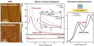
The two-step method (low-temperature deposition and room-temperature annealing) used by the authors in growing epitaxial aluminum films with the aid atomic force microscopy and x-ray diffraction indicated a far less root-mean-square value of roughness compared with polycrystalline aluminum films deposited at room temperature using regular evaporation methods.
The images of plasmonics nanostructures obtained by scanning electron microscopy, fabricated by focused-ion-beam milling showed a better visibility and straight slot edges fabricatied on the epitaxially grown aluminum film compared to the thermally deposited polycrystalline aluminum films in which had slot edges with dissimilar shapes and structural defects.
The authors however, discovered that at higher deposition rates, certain features which were achieved in the kind of time-consuming, two-step process grown aluminum film could also be retained with aluminum films deposited at room temperature. This can cover up for the time spent in a two-step process.
From spectroscopic ellipsometry measurements, results indicate that the oxidation of aluminum when exposed to ambient conditions did not change its surface morphology over a certain period of time. The irregularities found in the single-crystalline aluminum film using the two-step process were also lower than that of the thermally deposited polycrystalline aluminum film. Likewise, the intrinsic loss of aluminum with the use of the two-step method was almost twice as low compared to the extensively reported Palik’s value of polycrystalline aluminum films.
Outcomes from the uniqueness test verified that the derived fitting model coupled with the provision of valid intrinsic optical constants found by the authors can be extensively applied for plasmonic applications, e.g., providing a better theoretical limit to the performance of plasmonic devices.
The derived intrinsic optical constants of the epitaxial aluminum film guarantee a more accurate theoretical predictions in future designs of such devices. According to Dr. Fei Cheng who is the first author of this paper, “To the best of our knowledge, this is the first time to determine the intrinsic dielectric function of pristine Al.”
As reported by a perspective article on this work in the same issue of ACS Nano, “These results provide data that are essential for accurate agreement between theory and experiment for Al plasmonic nanostructures, placing this earth-abundant metal on sound footing as a new and highly promising material for sustainable plasmonics by design.”

Journal References
Cheng, F.1, Su, P.H.1, Choi, J.1, Gwo, S.2, Li, X.1, Shih, C.K.1, Epitaxial Growth of Atomically Smooth Aluminum on Silicon and Its Intrinsic Optical Properties, ACS Nano 10 (2016) 9852-9860.
Christopher J. DeSantis, Michael J. McClain, and Naomi J. Halas Walking the Walk: A Giant Step toward Sustainable Plasmonics, ACS Nano, 10 (2016), 9772−9775.
[expand title=”Show Affiliations”]- Department of Physics, University of Texas at Austin , Austin, Texas 78712 United States
- Department of Physics, National Tsing-Hua University , Hsinchu 30013, Taiwan
Go To ACS Nano