Significance Statement
High-speed integrated circuits are valuable components in high-speed and large-capacity information systems that have taken center stage in the human life. In order to improve the operating speeds of the integrated systems while reducing their power dissipation, optical interconnections have been introduced into these circuits. However, the scale of feasible optical devices that are used is much larger than that of the integrated electronic devices in these circuits, because the propagating light cannot escape the diffraction limit, while the waveguide structures are complex.
Plasmonic devices are simple structures which are not restricted by the light diffraction limit. These devices have, therefore, attracted considerable research attention and have simulated global developments initiatives.
Researchers lead by Professor Mitsuo Fukuda from Toyohashi University of Technology in Japan developed plasmonic and electronic device-based integrated circuits. In their work, they presented a new integrated plasmonic circuit comprising multiple plasmonic waveguides, a detector, and two metal–oxide–semiconductor field-effect transistors. Their work is now published in peer-reviewed journal, Solid-state Electronics.
Plasmonic devices were introduced to enable the high density monolithic integration of optical and electronic devices on a silicon substrate. The researchers opted for plasmonic devices that were simple structures which would be fabricated easily and operate in a wavelength range at which silicon is transparent to avoid accidental crosstalk caused by absorption at the substrate or in the electronic devices themselves.
The proposed integrated circuits were made of silicon, metals and silicon oxide using conventional silicon processes and no other materials or devices were used in these circuits. The plasmonic devices were designed based on the proposed concept using the finite-difference time-domain method and computer-aided design.
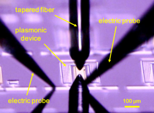
After the plasmonic design process, the device was fabricated by focused ion beam milling of gold film that was deposited on the silicon substrate. The plasmonic waveguides and the detector were monolithically integrated along with a metal–oxide–semiconductor field-effect transistor-based electronic circuit on the n-type silicon substrate.
The integrated circuit performance was investigated from the viewpoints of its static and dynamic characteristics. Static characteristics were assessed by observing circuit operations under continuous-wave incident light. The electrical signal that was converted from the surface plasmon polariton drove the metal–oxide–semiconductor field-effect transistors, and output current and voltage were monitored using an electrometer.
It was demonstrated that electronic devices such as metal–oxide–semiconductor field-effect transistors can be driven using surface plasmon polaritons with energies corresponding to the wavelengths at which silicon is transparent.
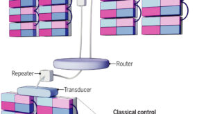
This indicates that the required optical devices, which are much larger than the corresponding electronic devices and have complex structures, can be monolithically integrated in the form of plasmonic devices on the same silicon substrate as the electronic devices using simple structures.
The circuits were fabricated using conventional silicon processes without the use of any other devices or materials. The connections between these devices were made using only metal wires or metal wire that were covered by dielectric films. On these metal wires, the surface plasmon polaritons can carry coherent plasmonic signals and intensity signals at the speed of light. These outcomes will definitely open the path towards development of new photonic integrated circuits composed of plasmonic and electronic devices.


Journal Reference
H. Sakai1, S. Okahisa1, Y. Nakayama1, K. Nakayama1, M. Fukuhara2, Y. Kimura1, Y. Ishii1, and M. Fukuda1. Plasmonic and electronic device-based integrated circuits and their characteristics. Solid-State Electronics, volume 125 (2016), pages 240–246.
[expand title=”Show Affiliations”]- Department of Electrical and Electronic Information Engineering, Toyohashi University of Technology, 1-1 Hibarigaoka, Tempaku-cho, Toyohashi, Aichi 441-8580, Japan
- Japan Society for the Promotion of Science, 8 Ichiban-cho, Chiyoda, Tokyo 102-8472, Japan
Go To Solid-State Electronics