
Significance
Graphene materials have found a wide range of applications in various fields such as electronics as a result of their favorable electrical, chemical and mechanical properties. However, their functionalities and properties can be compromised by nanodefects problems such as the grain boundaries. Due to their 2-dimensional layer, they can be formed through various processes one of them being chemical vapor deposition. During such processes, some of the defects observed in the graphene are formed. Grain boundaries, for example, are formed as a result of the intersection of the islands structures emanating from the multiple sites during the nucleation process of the chemical vapor deposition.
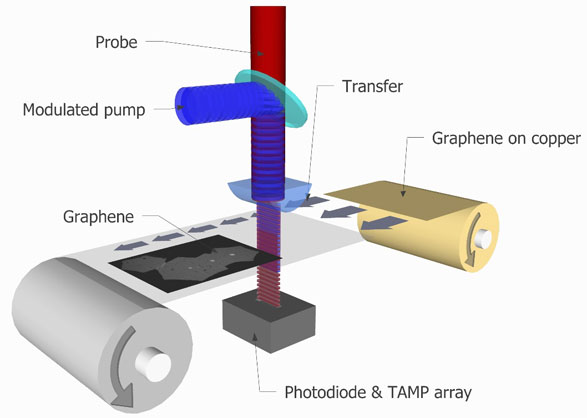
To understand the formation and effects of the grain boundaries on the properties and functionality of the graphene materials, several methods have therefore been developed to help in the imaging of the grain boundaries. Such methods apply different principles in imagining the defects. Transient absorption technique, a graphene measuring method depends on the pump to excite the electrons from the valence band to the conduction band. With the rapid growth and demand for graphene materials, large manufacturing processes are inevitable. Thus, transient absorption techniques can be modified to enable imaging of the grain boundaries and other defects in the materials at high and convenient speeds.
Boston University researchers: PhD student Kai-Chih Huang, Professor Chen Yang, Professor Ji-Xin Cheng and Postdoctoral fellow Chien-Sheng Liano in collaboration with PhD student Jeremy McCall and Technician Gregory Eakins at Purdue University together with Professor Pu Wang from Beihang University in China developed a new method based on the use of transient absorption microscopy for imaging the grain boundaries and other nanodefects in graphene materials. They also investigated the imaging speeds that could be used for the characterization of the nanodefects during the manufacturing processes of graphene such as the large area chemical vapor deposition. The research work is currently published in the journal, Nano Letters.
To significantly improve the functionality of the experimental setup regarding the spatial speeds, the authors used line-illuminated scanning method rather than the conventional raster scanning technique. They also used a tuned amplifier and photodiode array detection system invented by Ji-Xin Cheng and coworkers.
The authors observed that line-illumination scanning method increased the imaging speed of the transient absorption for instance by 1000 frames for every second. This is far much higher than the other speeds obtained in the previous studies through other methods. The system was also capable of characterizing the graphene nanodefects depending on the transient decay rate.
The research team successfully developed a new method that enables the detailed study and characterization of the grain boundaries of the graphene materials depending on the different available manufacturing techniques. For instance, the excellent speeds achieved in this work can resolve some of the defects associated with the grain boundaries like the surface wrinkles, surface coverage, and the grain numbers. Besides, their system is versatile and flexible and hence not limited to graphene and be used to study for example biological systems.

Reference
Huang, K., McCall, J., Wang, P., Liao, C., Eakins, G., Cheng, J., & Yang, C. (2018). High-Speed Spectroscopic Transient Absorption Imaging of Defects in Graphene. Nano Letters, 18(2), 1489-1497.
Go To Nano Letters
