
Significance
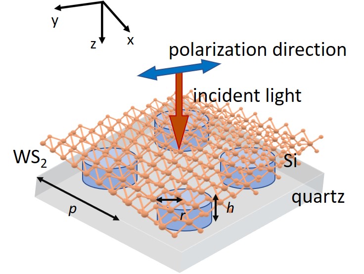
To this account, new research paper published in Optics Letters and conducted by Dr. Dingwei Chen and Professor Junichi Takahara from the University of Osaka, the researchers developed two key metasurface models: a Si Mie-resonant array supporting either electric or magnetic dipole modes, and a Huygens Si metasurface achieving degenerate critical coupling (DCC) where both resonances overlap. The first model established coherent exciton–photon coupling and revealed the formation of Miexcitons with moderate Rabi splitting (~42 meV). The second model amplified this effect through dual-mode interference, enhancing the coupling to 57 meV and achieving near-unity absorption (∼0.90). The team constructed a crystalline Si metasurface composed of cylindrical Mie resonators with tunable radius (70–120 nm), height (50–130 nm), and lattice period (2r + 110 nm). A monolayer WS₂ film was transferred onto this array, and its absorption response was simulated using the finite-difference time-domain (FDTD) method with experimentally derived optical permittivity data. The calculated absorption was obtained as one minus the sum of reflectivity and transmissivity, enabling extraction of intrinsic WS₂ absorption even in the presence of a lossy substrate. The authors found in their initial simulations that suspended WS₂ exhibited a peak absorption of ~10% at 615 nm, while WS₂ supported on Si dropped to ~4%. However, when coupled with the Si metasurface, distinct resonance phenomena emerged. By tuning the resonator radius to around 80 nm (period 270 nm, height 110 nm), the magnetic dipole (MD) resonance coincided with the WS₂ excitonic peak, resulting in a total absorption of 0.47, of which 0.27 originated from the excitonic contribution. The enhanced local tangential electric field associated with the MD mode strengthened light–exciton interactions, although the MD resonance itself was partially suppressed due to WS₂-induced perturbation. They observed a more pronounced effect under electric dipole (ED) coupling. When the metasurface was adjusted to d = 320 nm, r = 105 nm, and h = 105 nm, the system displayed an anticrossing feature characteristic of exciton-induced transparency (EIT), signifying the formation of hybrid exciton–photon modes—Miexcitons. The Rabi splitting energy (Ω ≈ 42 meV) indicated intermediate coupling, sufficient to redistribute the electromagnetic density of states and elevate WS₂ absorption to 0.55. The authors also found that engineered degenerate critical coupling (DCC) conditions by overlapping the ED and MD resonances through fine control of resonator dimensions (d = 334 nm, r = 112 nm, h = 92 nm). Under this configuration—termed the Huygens Si metasurface—both resonances coherently interfered, intensifying the local electromagnetic field near WS₂. The resulting spectrum showed dual peaks at 610 and 628 nm, each approaching unity absorption (~0.90–0.93). The extracted excitonic absorption reached 0.70, corresponding to an 18-fold improvement compared to WS₂ on a bare Si substrate. The enhanced Rabi splitting of 57 meV confirmed that DCC amplified coherent coupling by matching optical and nonradiative losses. Remarkably, absorption remained above 60% even at incidence angles up to 30°, which highlights robustness and potential scalability for practical photonic integration.
In conclusion, the new study by Chen and Takahara developed new systems that demonstrate a scalable, all-dielectric strategy for manipulating light–exciton interactions in 2D semiconductors and shows how geometric control within a silicon metasurface can overcome the intrinsic absorption limits of atomically thin TMDCs. They established a regime where excitons and photonic modes hybridize coherently, forming a coupled state that facilitates energy exchange rather than loss by exploiting the interplay of electric and magnetic Mie resonances. We believe the implications goes beyond WS₂ because Huygens metasurfaces can be tuned across visible frequencies through simple adjustments in resonator dimensions, this design can be generalized to other TMDCs such as MoS₂, MoSe₂, and WSe₂. Achieving degenerate critical coupling (DCC) enables both high absorption and enhanced field localization without relying on metals or cryogenic environments. Such versatility positions this platform as a practical route for realizing energy-efficient photodetectors, modulators, and exciton-based sensors operating at room temperature. Additionally, since the metasurface relies on crystalline Si—a CMOS-compatible material—the approach aligns naturally with semiconductor manufacturing, which suggest a straightforward integration path for on-chip photonic circuits.
What stands out most in the new study is the depth of physical understanding it brings to exciton–photon interactions. When excitons couple to overlapping electric and magnetic dipole resonances, the authors show that the local photonic density of states rises dramatically, creating a region where energy exchange is efficient but not wasteful. This intermediate regime is crucial—it strengthens the coupling without tipping into the dissipation that typically plagues plasmonic or cavity-based systems. The ability to hold that balance, to extract the benefits of strong coupling without the losses, explains why the observed enhancement approaches an eighteen-fold increase compared to conventional substrates, an exceptional result for any room-temperature 2D material. Additionally, the implications are wide-ranging. Devices built on this principle could absorb and convert light far more effectively, all while remaining just a few atoms thick. More intriguingly, the link they draw between field symmetry, the overlap of electric and magnetic dipole modes—and excitonic coherence offers a conceptual toolkit for engineering metasurfaces that do more than passively interact with light. They could, in principle, shape exciton behavior itself. Looking forward, this idea naturally extends into areas such as polaritonic logic, low-power photonic computing, and even quantum information processing, where control over coherent light–matter coupling is indispensable. Ultimately, the new work of Dr. Dingwei Chen and Professor Junichi Takahara replaces material layering with geometric results and shows that the architecture of light itself can be designed as the active element.


REFERENCE
Chen D, Takahara J. Enhancement of excitonic absorption in WS2 mediated by Huygens Si metasurfaces. Opt Lett. 2025;50(13):4246-4249. doi: 10.1364/OL.562981.
Opt Lett.