 Advances in Engineering Advances in Engineering features breaking research judged by Advances in Engineering advisory team to be of key importance in the Engineering field. Papers are selected from over 10,000 published each week from most peer reviewed journals.

Silicon carbide (SiC) is an important semiconductor for quantum technologies because it can host atomic defects known as color centers. These defects have optical and spin properties that make them suitable for quantum information processing and communication. Some emit light at wavelengths compatible with optical fiber networks, and their quantum states can remain coherent even at room temperature. However, producing individual color centers at precisely defined locations without damaging the surrounding crystal remains a technical challenge.
Conventional methods for creating these defects include electron and ion irradiation, which can introduce unwanted lattice damage and affect their optical and spin properties. Femtosecond laser writing provides another way to generate localized defects within a crystal. Short laser pulses deposit energy into a small volume, creating structural changes that may lead to defect formation. Controlling this process requires a better understanding of how the deposited energy travels through the crystal and how the lattice responds immediately after excitation.
Laser-induced energy transport involves different types of lattice motion. Coherent strain waves propagate through the crystal as organized mechanical disturbances, carrying energy away from the excited region. Local heating also produces structural distortions associated with incoherent atomic motion. These responses occur on very short timescales and can overlap spatially, making them difficult to distinguish experimentally.
X-ray diffraction can detect changes in crystal structure, but conventional measurements generally average the response over a relatively large volume. This makes it difficult to determine whether a measured change originates near the laser-excited surface or deeper inside the material. Measurements that combine high spatial resolution with ultrafast timing are needed to follow how these processes develop independently.
In a recent research paper published in ACS Nano, Kumar Neeraj, Matthew J. Highland, Tao Zhou, Burak Guzelturk, Donald A. Walko, Nathan C. Flanders, Nazar Delegan, F. Joseph Heremans, Martin V. Holt, Stephan O. Hruszkewycz, and Haidan Wen from Argonne National Laboratory developed a depth-resolved, time-resolved X-ray nanodiffraction technique to investigate energy transport in silicon carbide. Their approach was designed to distinguish rapidly propagating strain waves from longer-lasting structural distortions near the excited surface, providing a three-dimensional view of the crystal’s response to laser excitation.
Experiments and Findings
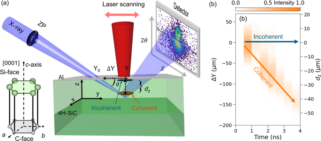
The investigation used a single crystal of 4H-SiC coated with a 60 nm aluminum layer. The aluminum served as a transducer, absorbing energy from a femtosecond laser pulse and generating a mechanical strain response in the underlying silicon carbide. This arrangement allowed the team to study how a controlled disturbance traveled into the crystal.
The measurements were carried out at the Advanced Photon Source using a tightly focused X-ray beam. By varying the delay between the laser excitation and the X-ray pulse, the team recorded structural changes at different times after excitation. Moving the laser position relative to the X-ray beam provided information about the depth and lateral location of the lattice response.
An unexpected observation emerged from the diffraction measurements. Laser excitation increased the X-ray diffraction intensity across the angular range surrounding the SiC Bragg peak, rather than producing the peak shift commonly associated with uniform lattice expansion or compression.
The team investigated this behavior by measuring the angular distribution of the diffracted intensity before and after excitation. The diffraction peak became broader, indicating that the crystal contained a distribution of local lattice strains. The focused X-ray beam had a relatively large angular convergence, meaning that only a small fraction of its incident wave vectors initially satisfied the diffraction condition of the undisturbed crystal. Following excitation, lattice distortions broadened the range of angles that could contribute to diffraction, increasing the measured intensity.
Numerical simulations provided further support for this interpretation. The calculated strain profile contained both tensile and compressive components, with strain magnitudes on the order of 10⁻³. Simulating the diffraction response using this profile reproduced the experimentally observed peak broadening. The agreement indicated that simultaneous lattice expansion and contraction contributed to the diffraction changes, even though the average peak position remained nearly unchanged.
The next question was whether the intensity changes reflected a single relaxation process or several different forms of lattice motion. To investigate this, the team compared measurements made at the center of the Bragg peak with measurements taken at slightly different diffraction angles.
The relaxation behavior differed considerably between these conditions. At the Bragg peak, the diffraction intensity decreased with a characteristic relaxation time of approximately 0.26 ns, compared with about 1 ns on either side of the peak. These differences were linked to the distinct structural processes detected at each angle. The rapid response at the Bragg condition was associated with a coherent strain pulse traveling through the crystal and leaving the X-ray-probed region. The slower response away from the peak was attributed to incoherent structural distortions associated with localized heating and strain variations near the aluminum–silicon carbide interface.
The temporal development of the diffraction signal supported this distinction. At the Bragg condition, the intensity increased over approximately 0.5 ns as the strain pulse entered the probed volume. Away from the Bragg peak, the response developed more rapidly, within approximately 0.2 ns, a timescale limited by the X-ray pulse duration.
To directly observe the spatial behavior of these components, the team collected diffraction maps at successive time delays and different positions of the laser beam. Measurements at the Bragg condition captured a feature that moved progressively deeper into the silicon carbide. Tracking its position gave a propagation velocity of approximately 11.4 ± 0.7 μm/ns, consistent with the longitudinal acoustic velocity of 4H-SiC. This provided direct evidence that the rapidly relaxing signal originated from a coherent acoustic strain wave.
In contrast, measurements away from the Bragg condition detected a structural response that remained close to the aluminum–silicon carbide interface and gradually weakened. Its lateral width increased with time, indicating that the affected region extended beyond its initial position. The observed broadening was greater than expected from thermal diffusion alone, suggesting that surface acoustic waves might also contribute.
Engineering Significance
The research establishes a way to distinguish different energy transport processes within a bulk semiconductor by combining depth-sensitive X-ray imaging with measurements at carefully selected diffraction angles. This distinction matters because structural changes that occur simultaneously after laser excitation do not necessarily share the same physical origin or relaxation behavior.
The angular dependence of the diffraction signal is especially useful. Measurements at the Bragg condition are more sensitive to coherent lattice motion associated with long-range crystalline order. Measurements away from this condition provide greater sensitivity to localized strain variations and structural disorder. Selecting different diffraction angles makes it possible to investigate these responses separately without changing the material or excitation conditions.
Another important contribution is the ability to connect diffraction measurements with the physical location of a disturbance inside the crystal. Conventional time-resolved diffraction measurements often combine structural responses from different depths. The nanofocused X-ray approach provides additional spatial information, making it possible to follow a propagating acoustic wave and distinguish it from structural changes that remain near an interface.
This capability has implications for understanding laser processing of silicon carbide, including the formation of color-center defects used in quantum devices. The balance between energy carried into the crystal by coherent strain waves and energy retained near the excitation region through local lattice distortions may influence the structural changes produced by laser writing.
The experiments examined reversible lattice responses generated through an aluminum transducer rather than directly observing permanent defect formation. Extending the measurement strategy to irreversible laser-induced changes could provide further information about the conditions associated with controlled defect creation.



Reference
Neeraj K, Highland MJ, Zhou T, Guzelturk B, Walko DA, Flanders NC, Delegan N, Heremans FJ, Holt MV, Hruszkewycz SO, Wen H. Depth-Resolved X-Ray Nanoimaging of Coherent and Incoherent Energy Transport in Silicon Carbide. ACS Nano. 2026;20(17):12850-12858. doi: 10.1021/acsnano.5c20241.