Significance Statement
Fresnel reflection occurs at the interface between two media with different refractive indices. In most of the materials used in mid-infrared (IR) or far-IR applications such as germanium (Ge), zinc sulfide (ZnS), and zinc selenide (ZnSe), very high reflectance results from their high refractive indices, which significantly degrade device performance. Single-layer antireflection coatings (ARCs) exhibit reduced reflection by their interference principle, however, it can only works in a narrow wavelength range. For broadband antireflection in the IR region, multi-layer stacks with thickness of few micrometers are needed, which causes increased fabrication time and cost. Moreover, thin film technology has inherent problems such as adhesion, thermal mismatch, and stability of thin film stacks.
On the other hand, the studies on biomimetic subwavelength structures, originally inspired by the excellent antireflective capability of corneal of night active insects, have been developing rapidly. The basic idea is that the nanostructured coating-materials are capable of creating a gradient refractive index profile due to their tapered morphology, and consequently forms their unique broad wavelength antireflection property. In recent years, various nanofabrication techniques and new antireflective materials have emerged. Nevertheless, reported works mainly focus on the AR properties in the visible and near-IR wavelength ranges.
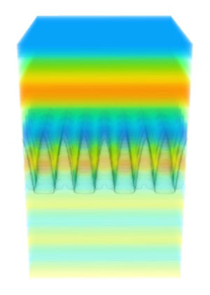
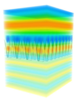
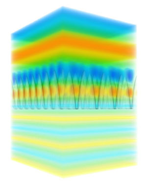
Our team have recently introduced antireflective microstructures on ZnS substrates for mid- and far-infrared applications. To enhance the AR properties, parabola shape with a 6-fold hexagonal symmetry, which provides linear graded refractive index profile, was used. By considering the fabrication procedure and tolerance, we investigated optimum geometry of ZnS antireflective microstructures with parabola shape for mid- and far-IR applications. Also, the effects of the heights and periods on the reflectance were analyzed. The ZnS antireflective microstructures with optimized geometry can be used to applications including night vision, thermal imaging, motion sensors, astronomy, and forward looking infrared (FLIR) technology. Furthermore, it can be extended for other applications such as photovoltaics and electromagnetic wave sensing by using different materials and changing the periods and heights.

Journal Reference
Optical and Quantum Electronics, 2015, Volume 47, Issue 6, pp 1503-1508.
Y.J. Yoo1,K. S. Chang2, S. W. Hong 3, Y. M. Song1
[expand title=”Show Affiliations”]- Department of Electronics Engineering, Pusan National University, 2 Busandaehak-ro 63beon-gil, Geumjeong-gu, Busan, 609-735, Republic of Korea
- Center for Analytical Instrumentation Development, Korea Basic Science Institute, 169-148 Gwahak-ro, Yuseong-gu, Daejeon, 305-806, Republic of Korea
- Department of Cogno-Mechatronics Engineering, Pusan National University, 2 Busandaehak-ro 63beon-gil, Geumjeong-gu, Busan, 609-735, Republic of Korea
Abstract
We present broadband antireflective microstructures (AMSs) for high-performance imaging systems in mid- and far-infrared wavelength ranges. Diffraction efficiencies of antireflective microstructures on ZnS substrates were calculated using a rigorous coupled wave analysis method. The results show the effect of height, period, and shape of antireflective microstructures on the reflection characteristics. We also discuss the optimum geometry of AMSs by considering fabrication tolerances.
Go To Optical and Quantum Electronics