
Significance Statement
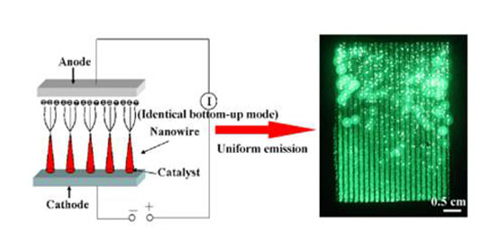
Boron nanowire (BNW) arrays have been considered as an ideal optoelectronic nanomaterial due to their outstanding electric and mechanical properties. But in regards of their field emission (FE) and high-temperature device applications, they can hardly been grown in identical growth mode that badly affects the uniformity of their physical behaviors. It is noted that different physical performances of nanostructures on the same substrate is a common phenomenon in experiments, which may result from different growth modes of the nanowires. The existence of this problem has inhibited their rapid developing in nanodevice applications, and thus becomes a big challenge for most researchers. To solve this problem, a simple way is reported to control the growth of Boron nanowire arrays in an identical bottom-up growth mode. The Boron nanowire arrays after our modulation were found to exhibit more excellent field emission properties than the Boron nanowire (in different growth modes) prepared by other ways, which may provide a helpful reference to fabricate various nanostructure arrays in identical growth mode.
This work (presented in “Small”) is accomplished by Liu et al. (State Key Laboratory of Optoelectronic Materials and Technology at Sun Yat-sen University in China) and their collaborators (Inorganic Nanostructured Materials Group at National Institute for Materials Science in Japan).
Small, Volume 10, Issue 4, pages 685–693, 2014.
Fei Liu1,2,*, Haibo Gan1, Dai-Ming Tang3,Yunzhe Cao1, Xiaoshu Mo1, Jun Chen1,Shaozhi Deng1, Ningsheng Xu1, Dmitri Golberg4 , Yoshio Bando2
- Address State Key Laboratory of Optoelectronic Materials and Technologies, Guangdong Province Key Laboratory of Display Material and Technology, and School of Physics and Engineering, Sun Yat-sen University, Guangzhou, PR China.
- Inorganic Nanostructured Materials Group, MANA, National Institute for Materials Science, Tsukuba, Ibaraki, Japan.
- International Center for Young Scientists (ICYS), National Institute for Materials Science, Tsukuba, Ibaraki, Japan.
- Nanotube Group, MANA, National Institute for Materials Sciences, Tsukuba, Ibaraki, Japan.
Abstract
Boron nanowires (BNWs) are considered as an ideal optoelectronic nanomaterial, but controlling them in identical growth mode and large-area patterns is technically challenging. Here, large-scale Boron nanowires patterns with a uniform base-up growth mode are successfully fabricated by choosing Ni film as the catalyst. Moreover, they exhibit low turn-on field (4.3 V/um) and excellent field emission uniformity (88%).
© 2013 WILEY-VCH Verlag GmbH & Co. KGaA, Weinheim
