
Significance Statement
All-optical method for quantifying thermal conductivity in individual silicon nanowires using pump-probe microscopy
Management of thermal energy is an important concern in the design of nanoelectronic devices. Understanding of the thermal characteristics of individual components is crucial for designing the properties of the overall system, however it is difficult to measure the thermal conductivity of such small structures, and even more challenging are variations in the conductivity within a single structure. We have developed an ultrafast microscopic technique which can measure the thermal conductivity in localized regions of a nanostructure in an all-optical, contact-free configuration.
In pump probe microscopy a pump pulse excites free carriers in a localized region of a silicon nanowire. The carriers thermalize to the band edge within 100s of femtoseconds depositing ~2 eV of energy into the lattice as heat. A probe pulse interacts with the sample at a specific delay. The presence of free carriers in the wire renders it more transparent to the probe increasing the probe intensity, while an increase in thermal energy in the wire decreases intensity. By pumping in one location and probing in another, we can observe the movement of free carriers and thermal energy within a nanowire.
Free carrier dynamics (i.e. recombination and diffusion) and thermal transport are measured in both the suspended and substrate-supported sections of a NW suspended across a narrow (~8 μm) channel etched into a quartz slide. While the substrate has no effect on the recombination time or diffusion length, it does significantly impact the thermal relaxation properties of the NW. Thermal energy deposited into the lattice by the laser pulse dissipates within ~10ns through coupling to the substrate, while in suspended regions it persists for over 100ns.
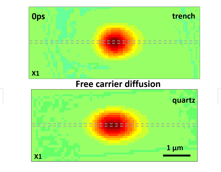
Figure legend: By pumping the wire in one location and scanning the probe beam across the sample we can image the spatial distribution of charge carriers and thermal energy at various delays.
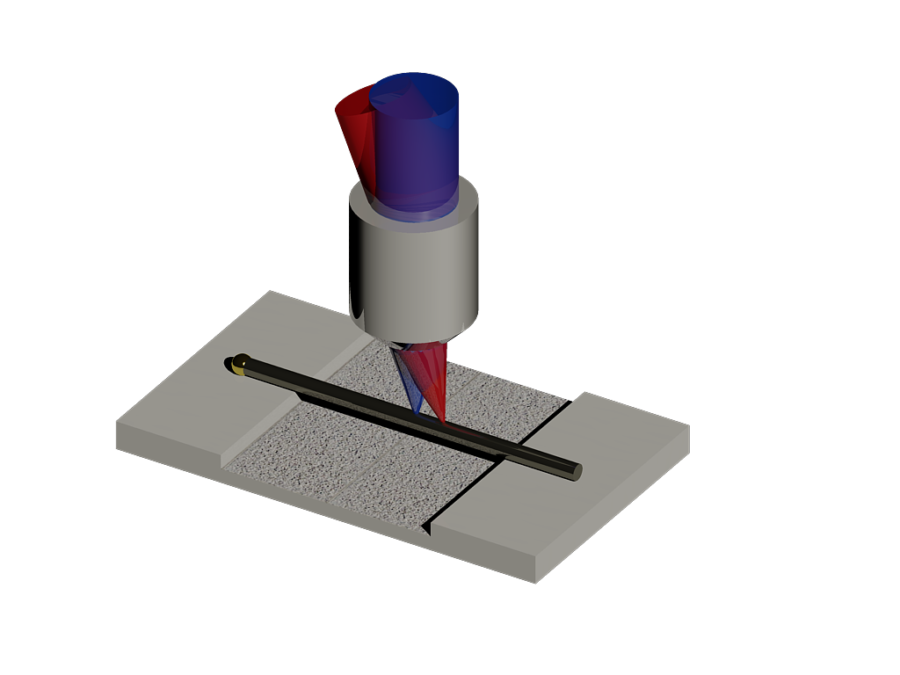
Figure Legend: Spatially separated pump probe microscopy allows us to image the spread of free charge carriers (red) from 0 ps – 267 ps, by which time they have all recombined. The spread of thermal energy (blue) through the wire is observed until the wire cools. Dissipation of thermal energy takes about 25 ns in the portion of the wire in contact with the substrate, while it persists for over 100 ns in the suspended segment. The rates of free carrier diffusion are the same in both sections, as are the thermal conductivities.
Journal Reference
Department of Chemistry, University of North Carolina at Chapel Hill, Chapel Hill, North Carolina 27599-3290, United States.
Abstract
Thermal management is an important consideration for most nanoelectronic devices, and an understanding of the thermal conductivity of individual device components is critical for the design of thermally efficient systems. However, it can be difficult to directly probe local changes in thermal conductivity within a nanoscale system. Here, we utilize the time-resolved and diffraction-limited imaging capabilities of ultrafast pump–probe microscopy to determine, in a contact-free configuration, the local thermal conductivity in individual Si nanowires (NWs). By suspending single NWs across microfabricated trenches in a quartz substrate, the properties of the same NW both on and off the substrate are directly compared.
We find the substrate has no effect on the recombination lifetime or diffusion length of photogenerated charge carriers; however, it significantly impacts the thermal relaxation properties of the NW. In substrate-supported regions, thermal energy deposited into the lattice by the ultrafast laser pulse dissipates within ∼10 ns through thermal diffusion and coupling to the substrate. In suspended regions, the thermal energy persists for over 100 ns, and we directly image the time-resolved spatial motion of the thermal signal. Quantitative analysis of the transient images permits direct determination of the NW’s local thermal conductivity, which we find to be a factor of ∼4 smaller than in bulk Si.
Our results point to the strong potential of pump–probe microscopy to be used as an all-optical method to quantify the effects of localized environment and morphology on the thermal transport characteristics of individual nanostructured components.
Copyright © 2015 American Chemical Society.
