Significance
The most common practice for performing accurate analysis of surface topography involves the utilization of both scanning electron microscopy and scanning probe microscopy. A combination of the two modalities has been observed to have abundant advantages, such as localization, navigation etc. The past two decades has seen various approaches purposed to integrate atomic force microscopes into scanning electron microscopes for application in nano-electronic transport processes and cathode-luminescence based studies. Furthermore, the combination of a scanning tunnel microscope with a microwave resonator has borne the scanning microwave microscope which has found numerous applications. Unfortunately, using this technique to extract information of the complex quantities of conductivity, permittivity, and permeability has been a challenge. Therefore, it is imperative to comprehend both the interaction of the incident electromagnetic wave and the physics of the sample so as to obtain the quantitative data from the measurements.
To this note, University of Oldenburg researchers at the Department for Computing Science: Dr. Olaf C. Haenssler and Professor Sergej Fatikow in collaboration with Professor Didier Theron, of CNRS-IEMN in Lille, France employed the integrated scanning microwave microscope technique to simultaneously extract multimodal nanoscale specimen information. The combination of multiple imaging techniques allowed them to obtain complementary and unique datasets of the samples under investigation. Their work is currently published in Journal of Vacuum Science & Technology B.
Briefly, the research method employed involved the use of an atomic force microscope based on a compact optical interferometer to perform imaging of surface topographies and a scanning microwave microscope to record electromagnetic properties in the microwave frequency domain up to 20 GHz at the same time and spot. In addition, an open-source software framework, which was tailored for vision-based automation by nanorobotics, was used to control the instrument.
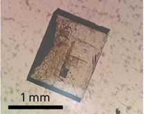
The authors observed that the capacitance approximation formulas for rectangular metal-oxide-semiconductor structures in literature deviated from the RF simulation results obtained by more than 20%. Moreover, the capacitance values in the considered area of 380 aF, showed strong contrast thereby proofing the concept. However, it was noted that smaller scaled features were not available at the time of preparation.
In summary the University of Oldenburg and CNRS-IEMN scientists successfully presented a hybrid technology developed by integrating several microscopy modalities which enabled them extract multiple information of sample surfaces by detection of electron, light, microwave interaction and atomic force. In general, a study of micro-scaled capacitors was undertaken so as to evaluate the developed instrumental platform and show the potential of the resulting multimodal technology. Altogether, their setup demonstrated here allows for simultaneously observation of the region-of-interest with scanning electron microscopy resolution, while imaging and characterization with evanescent microwaves and atomic forces.


Reference
Olaf C. Haenssler, Sergej Fatikow, Didier Theron. Multimodal imaging technology by integrated scanning electron, force, and microwave microscopy and its application to study micro-scaled capacitors. Journal of Vacuum Science & Technology B 36, 022901 (2018); doi: 10.1116/1.5006161
Go To Journal of Vacuum Science & Technology