
Significance Statement
Graphene, a single layer of carbon atoms forming a honeycomb lattice structure, has been considered as a wonder material for both scientific research and technological applications because of its unique electronic, thermal, magnetic and mechanical properties and its super-functional capabilities. Among various novel properties, the existence of a nontrivial topological phase (also known as the Berry phase) associated with each of the two inequivalent valleys in graphene is deemed as a unique component suitable for applications to quantum information technology and dissipation-free field effect transistors (FETs). However, such valleytronic applications can only be realized by either breaking the time-reversal symmetry or the inversion symmetry of graphene. The former may be achieved by inducing finite ferromagnetism in graphene, whereas the latter may be realized by gingerly aligning the honeycomb lattice of a monolayer of graphene with atomic precision on top of a monolayer of hexagonal boron nitride. However, neither approach is easily manageable for scale-up applications because of the small energy gaps involved in the aforementioned perturbations, which imply the requirement of low-temperature operation. The complicated material processing also imposes additional challenges on device fabrication in large quantity.
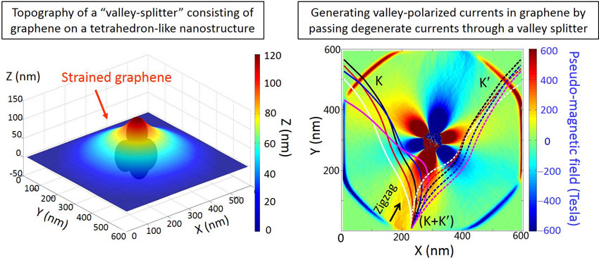
A recently developed single-step process for room-temperature PECVD growth of large-area, high-mobility and nearly strain-free graphene opens up a new paradigm for realizing graphene-based valleytronics when combined with modern nanoscale fabrication technology. Specifically, properly strained graphene at nanoscales can result in giant pseudo-magnetic fields that couple to the two inequivalent valleys with opposite signs. Therefore, controlled strain on perfect graphene can be tailored to yield the desirable electronic properties for valleytronic applications, and the strength and spatial distributions of the required strain may be induced by designing and then fabricating nanostructures on the substrates for graphene. In particular, the energy scale of the giant pseudo-magnetic fields could be so high that even room temperature operation would be feasible. The notion of nanoscale “strain engineering” of the gauge potential of graphene is the primary motivation of this article published in Acta Mechanica Sinica, which describes the theoretical foundation for strain engineering the electronic properties of graphene, demonstrates preliminary theoretical simulations and nanofabrication approaches to implementing the nanoscale engineering, and then provides experimental evidences for the manifestation of strain-induced giant pseudo-magnetic fields. Exemplifying valleytronic devices based on nanoscale strain engineering of graphene are also discussed.
While this article focused on nanoscale strain engineering of graphene for valleytronic applications, it should be considered as an example of a new paradigm of research that exploits the interesting interplay of structural, electronic, and topological properties of nano- and meta-materials. This type of endeavor is likely to open up new frontiers in scientific and technological expeditions that have not been envisioned before.


Journal Reference
Acta Mechanica Sinica, pp 1-13, February 2016.
N.-C. Yeh 1, C.-C. Hsu1, M. L. Teague1, J.-Q. Wan2, D. A. Boyd3, C.-C. Chen1
[expand title=”Show Affiliations”]- Department of Physics, Institute for Quantum Information and Matter, and Kavli Nanoscience Institute, California Institute of Technology, Pasadena, CA, 91125, USA
- Department of Physics, Fudan University, Shanghai, China
- Department of Physics, California Institute of Technology, Pasadena, CA, 91125, USA
Abstract
Structural distortions in nano-materials can induce dramatic changes in their electronic properties. This situation is well manifested in graphene, a two-dimensional honeycomb structure of carbon atoms with only one atomic layer thickness. In particular, strained graphene can result in both charging effects and pseudo-magnetic fields, so that controlled strain on a perfect graphene lattice can be tailored to yield desirable electronic properties. Here, we describe the theoretical foundation for strain engineering of the electronic properties of graphene, and then provide experimental evidence for strain-induced pseudo-magnetic fields and charging effects in monolayer graphene. We further demonstrate the feasibility of nano-scale strain engineering for graphene-based devices by means of theoretical simulations and nano-fabrication technology.
Go To Acta Mechanica Sinica
