
Structural color printing that implements micro or nanostructures to display various colors has developed reference to the advancement in nanotechnology. As opposed to conventional color printing methods that relied on inks, structural colors depend on the interaction of light with physical structures. Structural colors have appealing attributes in terms of color, chromaticity, resolution, chemical stability and being environmental friendly.
Regardless of the current development of this technique, structural color printing suffers low throughput as well as poor versatility in the production of large scale color patterns. Therefore, its practical applications are only limited to security features and in microscale nano-optical displays.
Conventional inkjet-based color printing implements inks based on pigments or dyes to print color patterns. Structural colors can also be inkjet-printed using inks comprised of nanostructured materials. Dr. Hao Jiang and colleagues from Simon Fraser University in Canada presented a convenient structural coloration method: molded ink on nanostructured surfaces. The technique was based on molding the shape of printed ink materials on top of surface-supported transparent polymer nanostructures to display structural colors. The work is published in peer-reviewed journal, ACS Nano.
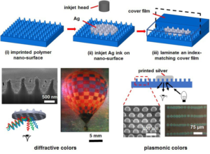
A transparent substrate was prepared by imprinting polymer nanostructures on a plastic sheet. The nanostructures were prepared to cover all of the printable area on the substrate. Silver nanoparticle ink droplets were then printed on the nanostructured surface through inkjet printing consistent with the user defined pattern.
In the molded ink on nanostructured surfaces, after a silver ink droplet dried into a solid silver thin-film, the silver was modified by the polymer nanostructures and, therefore, it gained structural colors. These colors were dictated by the geometries of the polymer nanostructures and rheological properties of the ink. After printing, the sample’s surface was laminated with a transparent index-watching cover to inactivate the unprinted nanostructures in order to display a transparent background.
In a bid to demonstrate the molded ink on nanostructured surfaces printing technique, the authors adopted polymer nanocone arrays on transparent polyethylene terephthalate sheet as substrate. After printing, the silver dot was a silver nanostructure immersed in the transparent polymer background. The nanostructure was found to have different surface profiles: a silver nanocone array on the top side, and a silver nanowell on the bottom. By adjusting the geometries of nanocones, diffractive colors and plasmonic colors were both achieved.
This study presented the concepts and the experimental results of molded ink on nanostructured surfaces printing based on inkjet on pre-fabricated surface-supported polymer nanostructures. Molded ink on nanostructures surfaces printing implements a single type of silver nanoparticle ink, halftone process to control the brightness of subpixels, additive color model to mix into a wide range of visual colors, and nanostructured substrates to print structural colors inexpensively. The technique developed by the authors allows for structural color images to be printed in a pattern-on-demand fashion with high throughput and can inspire novel designs of nanostructured substrates to enable plasmonic printing of large format images.
“The most appealing advantages of this technique are the high throughput and versatility. For example, any photo-sized structural color pattern can be printed in minutes using our technique, compared to a few days, or even weeks, using conventional nanofabrication tools”, said Dr, Hao Jiang.


Journal Reference
Hao Jiang, Sheida Alan, Haleh Shahbazbegian, Jasbir N. Patel, and Bozena Kaminska, Molding Inkjetted Silver on Nanostructured Surfaces for High-Throughput Structural Color Printing. ACS Nano, 2016, 10 (11), pp 10544–10554.
School of Engineering Science, Simon Fraser University, Burnaby, British Columbia V5A1S6, Canada.
Go To ACS Nano