Significance
Essentially, when two dissimilar metals or semi- conductor materials get into contact, they tend to generate a contact potential. Measurement of the contact potential difference (surface potential) and work functions of materials are important in analyzing their electronic structures and surface residual charges. Kelvin probe force microscopy (KPFM) is an imaging technique of atomic force microscopy which is commonly used to map the surface potential and work function at the nanoscale. Numerous variants of KPFM have been invented, however, these conventional KPFM variants are typically limited in their spatial resolution to 30−100 nm under ambient conditions. This is in conflict with the continuously decreasing size and increasing complexity of photoactive materials and semiconductor devices. As such, it is anticipated that future challenges in uncovering their nanometer scale electrical properties through KPFM will arise.
Therefore, to ensure that the KPFM technique remains a useful tool for analyzing emerging heterogeneous materials with nanoscale features, several improvements must be made to the technique. In light of this, researchers from the Department of Chemistry at Lehigh University, Pennsylvania, United States: Devon S. Jakob, Haomin Wang and led by Professor Xiaoji Xu, developed a novel KPFM technique based on the pulsed force mode of atomic force microscopy. Specifically, they invented pulsed force Kelvin probe force microscopy (PF-KPFM), which was based on an entirely new measurement paradigm not used in any existing amplitude-modulation KPFM and frequency-modulation KPFM techniques. Their work is currently published in the research journal, ACS Nano.
The proposed PF-KPFM approach is a single-pass technique that utilizes the intrinsic Fermi-level alignment between the atomic force microscopy tip and the conductive sample to generate signal without the need for an external oscillating voltage. A home-built circuit, which controls the resistance between tip and sample, was designed and implemented to completely avoid the necessity of an external AC voltage for signal generation. Spontaneous redistribution of electrons due to Fermi-level alignment occurs when the resistance is low. The team extracted the induced cantilever oscillations generated by the spatially separated charges and used them to obtain the cantilever oscillation amplitude and to derive the surface potential.
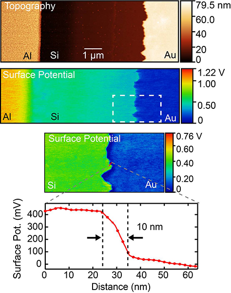
The research team reported that the PF-KPFM approach provided a spatial resolution of <10 nm for surface potential imaging in ambient conditions, which surpassed that of FM-KPFM under similar conditions by at least three times. Additionally, the PF-KPFM technique was shown to overcome many limitations of current KPFM techniques by bypassing the need for lift mode scans and minimizing unintended signal generation from the stray capacitance effect.
In summary, the study presented a widely applicable KPFM technique that operates entirely in the pulsed force mode of atomic force microscopy. To be precise, the presented PF-KPFM approach operates on a measurement paradigm based on the Coulomb force generated from intrinsic Fermi level differences, rather than from applying an external AC voltage. In a statement to Advances in Engineering, Professor Xiaoji Xu said that they anticipate the novel PF-KPFM will facilitate the characterization of photovoltaics, semiconductor structures, as well as nano- to microscale biological samples with residual charges. He further added that high spatial resolution measurements with PF-KPFM will facilitate advancing further studies directed at uncovering electrical properties for emerging photoactive materials, biological samples, and semiconductor devices.

References
Devon S. Jakob, Haomin Wang, Xiaoji G. Xu. Pulsed Force Kelvin Probe Force Microscopy. ACS Nano 2020, volume 14, page 4839−4848.
Devon S. Jakob, Haomin Wang, Guanghong Zeng, Daniel E. Otzen, Yong Yan, and Xiaoji G. Xu Peak Force Infrared – Kelvin Probe Force Microscopy Angewandte Chemie Int. Ed. DOI:10.1002/anie.202004211 (2020)
 Advances in Engineering Advances in Engineering features breaking research judged by Advances in Engineering advisory team to be of key importance in the Engineering field. Papers are selected from over 10,000 published each week from most peer reviewed journals.


