 Advances in Engineering Advances in Engineering features breaking research judged by Advances in Engineering advisory team to be of key importance in the Engineering field. Papers are selected from over 10,000 published each week from most peer reviewed journals.

Graphene is a single layer of carbon atoms whose electrical properties are closely related to its atomic structure. Although it is normally considered a nonpolar material, bending it at very small dimensions can alter the distribution of electrons and produce localized electrical polarization. Understanding this behavior is important for determining how mechanical deformation influences the electronic properties of two-dimensional materials.
One phenomenon responsible for this interaction is flexoelectricity, where a variation in mechanical strain across a material generates electrical polarization. Unlike piezoelectricity, which depends on the symmetry of a crystal, flexoelectricity can occur in materials that are otherwise electrically nonpolar. Its effects can become particularly pronounced in atomically thin materials because their flexibility allows them to develop sharp bends and strong strain gradients.
Graphene offers an interesting example because its electronic structure includes π orbitals that extend above and below the plane of carbon atoms. When the material bends sharply, the orientation and overlap of these orbitals change. At sufficiently small curvature radii, this redistribution of electron density can generate a quantum-mechanical contribution to flexoelectric polarization that differs from the conventional description based on mechanical deformation and charge separation.
Observing this effect experimentally has been difficult. Many studies involve bending graphene over distances much larger than the orbitals responsible for its electronic behavior. Measurements can also be affected by defects, substrate interactions, or external mechanical forces, making it challenging to isolate the intrinsic response. Another difficulty concerns structural symmetry. Even when strong curvature produces local electrical dipoles, their contributions can cancel if the overall geometry remains symmetric.
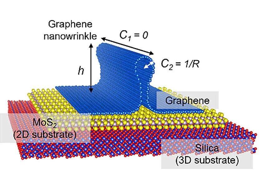
Graphene nanowrinkles offer a way to investigate these effects. They form when mechanical compression causes a graphene sheet to buckle into narrow, sharply curved structures. Their geometry combines large strain gradients with structural asymmetry, creating conditions in which curvature-induced electronic polarization may become measurable.
In a recent research paper published in Advanced Materials, a research team led by Professor Alan Dalton from the University of Sussex, Dr. Manoj Tripathi, Professor Pulickel Ajayan from Rice University, and Professor Vincent Meunier from Pennsylvania State University investigated quantum orbital flexoelectricity in self-assembled graphene nanowrinkles. The team combined nanoscale electrical measurements with atomic-level calculations to establish how extreme bending affects electron distribution and local electrostatic behavior.
Experiments and Findings
The researchers formed graphene nanowrinkles by placing graphene onto molybdenum disulfide (MoS₂), another atomically thin material. Differences in their mechanical properties and atomic structures create conditions that favor buckling under compression. Graphene can also slide more easily across MoS₂ than across silica, allowing small deformations to develop into pronounced wrinkles. Molecular dynamics simulations supported this process, showing that smaller wrinkles could merge into taller, standing-collapsed structures.
Atomic force microscopy revealed narrow features with estimated widths below approximately 5 nm and apex radii of curvature around 1–2 nm. These dimensions were obtained after correcting for the broadening introduced by the microscope tip. The researchers also used Raman spectroscopy to investigate strain across the graphene surface. The measurements indicated that compressive strain in relatively flat regions changes near the wrinkles, producing highly localized strain gradients.
The central question was whether these structures could generate polarization through changes in graphene’s electronic orbitals. Density functional theory calculations allowed the team to compare curved carbon structures with different geometries. In a symmetric, closed configuration, the redistribution of electron density remained balanced, preventing the formation of a net electrical dipole. An open graphene nanowrinkle behaved differently. Its asymmetric geometry displaced the centers of the electronic orbitals, producing a calculated polarization associated with the curved region.
This comparison established that curvature and symmetry play different roles. Sharp bending changes orbital interactions, while the asymmetric arrangement of the nanowrinkle allows the resulting electronic redistribution to produce a net electrical response.
To investigate whether this behavior could be observed experimentally, the team used Kelvin probe force microscopy to measure surface potential across flat and wrinkled graphene. The nanowrinkles exhibited work-function shifts relative to nearby regions, consistent with localized polarization affecting the electrostatic potential. The researchers interpreted these changes as evidence that curvature contributes substantially to the electronic response rather than the contrast arising solely from the substrate.
They performed conductive atomic force microscopy provided further information by measuring electrical current through individual wrinkles. Under an applied bias of 2 V, features with different heights produced similar currents of approximately 67 pA. This behavior suggested that the electrical response was associated more closely with the sharply curved apex than with the total height of the nanowrinkle.
The team then varied the applied voltage while repeatedly measuring the same regions. The current response was asymmetric under opposite bias polarities, and a characteristic threshold appeared near 1 V. Theoretical calculations predicted a corresponding electrostatic potential offset of approximately 1.2 V between curved and flat graphene. This agreement supported the proposed formation of a localized electrostatic junction caused by curvature-induced charge redistribution.
The calculations also indicated that the nanowrinkles did not open an electronic bandgap in graphene. Instead, their influence on electrical behavior arose from changes in the local potential and electron distribution.
The magnitude of the polarization was estimated using both theoretical and experimental approaches. Calculations yielded approximately 4 C/m², while the estimate derived from the measured electrical response was about 1 C/m². These values were several orders of magnitude greater than those reported for larger-scale flexoelectric systems, reflecting the intense curvature achievable in graphene nanostructures.
The experimental estimate relied on an approximate dipole model and geometric measurements close to the resolution limits of the microscopy technique. Nevertheless, the correspondence between the calculations and several independent electrical measurements provided consistent evidence for a strong quantum orbital flexoelectric contribution.
Engineering Significance
The new study establishes a connection between atomic-scale mechanical deformation and electronic polarization in graphene. Of particular importance is the distinction between conventional flexoelectricity and the quantum contribution arising from changes in the material’s electronic orbitals. At sufficiently small dimensions, bending affects not only the positions of atoms but also the spatial distribution of the electrons involved in bonding.
The findings provide a clearer understanding of how the geometry of a two-dimensional material can influence its electrostatic properties. A curved structure does not necessarily produce net polarization, even when the local electronic changes are substantial. The arrangement of the material must also allow those changes to create an uncompensated electrical dipole.
For materials engineering, the self-assembly of graphene nanowrinkles provides a practical means of studying this relationship without continuously applying an external mechanical force. Their formation through interactions with MoS₂ also suggests that substrate selection and mechanical mismatch could be used to influence the development of electrically active nanoscale features.
Another implication is related to the creation of local electrostatic junctions within a continuous graphene sheet. Rather than changing its chemical composition or opening a bandgap, sharply curved regions can modify the surrounding electronic potential. This provides a possible direction for investigating electronic structures in which mechanical geometry contributes to electrical functionality. Although integration into controlled device architectures remains a future step, the study identifies a physical mechanism that could inform the design of graphene-based and other two-dimensional material systems.



Reference
A. Iyengar, J. G. McHugh, J. P. Salvage, et al. “ Sub-Nanometer Curvature Unlocks Quantum Orbital Flexoelectricity in Graphene.” Advanced Materials 38, no. 57 (2026): e18224. https://doi.org/10.1002/adma.202518224