Significance Statement
The pressure to deliver fast, cost effective and high throughput fabrication techniques for excellent microfluidic analytical devices is rapidly mounting. This has been brought about by the rapidly increasing demand in the health and biomedical market for both in-vitro diagnostic devices and point-of-care testing devices, which are rapidly becoming vital tools for the development of advanced biomedical tests and treatments. Hindrances have often been encountered in the thermoplastic-based fabrication technologies, which are intrinsically suitable for large-scale mass production such as: hot embossing, thermoforming and injection moulding, but the costly mould fabrication process and time consuming process inhibit rapid turnaround of novel design. Conversely, recent technological advancements have tempted researchers on studying the applicability of microfluidic paper-based analytical devices for such similar purposes.
Zhibin Yan, Xiaoyang Huang and Chun Yang at Nanyang Technological University in Singapore, developed an easy low-cost rapid prototyping method for single-layer microfluidic polydimethylsiloxane devices with abrupt depth variations from micrometer to millimeter under non-clean-room conditions. Their research work is now published in Microfluids and Nanofluids (Springer).
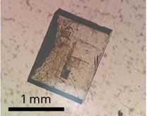
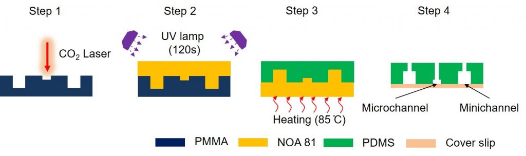
The research team began by engraving designed channels of distinct depths on polymethylmethacrylate plate so as to form a female mould. They then applied a layer of UV-curable polymer on the polymethylmethacrylate female mould so as to replicate the micro and mini-scale structures to form the master mould for a single Polydimethylsiloxane replica. The team then baked, on a hotplate, and cured the single layer of the polydimethylsiloxane replica. They then peeled off the replica from the UV-curable polymer male mould. Ultimately, the research team plasma bonded the polydimethylsiloxane replica with glass.
The authors observed that there was a slight reduction in the resolution in comparison with the conventional photolithography. Additional copper mask covered on polymethylmethacrylate plate and submerging the polymethylmethacrylate plate into aqueous environments during laser ablation procedure were also reported to improve the control of the channel shape. Alternatively, micro-milling was suggested for utilization as an affordable approach to replace the laser ablation in the first step of the proposed technique for the fabrication of the female polymethylmethacrylate mould since micro-milling was observed to yield micro-channels with well-controlled cross sections.
The fast prototyping method for single layer polydimethylsiloxane microfluidic device with abrupt depth variations was achieved by combining the laser ablation and a UV-curable polymer has been presented. The entire process can be completed in under two hours. This technique has proven that it can be applied to readily produce polydimethylsiloxane microfluidic devices with micrometer and millimeter structures in one step. Moreover, it is applicable in non-clean-room environs and does not require intricate and costly soft lithography equipment or etching processes. Despite the drop in the resolution paralleled with the conventional photolithography, the proposed technique provides a low-cost alternative for microfluidic study with limited microfabrication facilities and for fast evaluation of the proof-of-concept design.


Reference
Zhibin Yan, Xiaoyang Huang, Chun Yang. Rapid prototyping of single-layer microfluidic PDMS devices with abrupt depth variations under non-clean-room conditions by using laser ablation and UV-curable polymer. Microfluid Nanofluid (2017) 21:108
Go To Microfluid Nanofluid