Significance
Under ambient conditions, equiatomic zinc pnictides do not naturally form a free-standing monolayer whose atomic network remains both low in energy and resistant to distortion. That difficulty has kept ZnAs, ZnSb, and ZnBi in an uncertain position within the search for useful two-dimensional semiconductors: the bulk compounds already display unusual bonding, with electron-poor valence counts and multicenter connectivity, yet dimensional reduction has not produced a convincingly stable pristine sheet. For ZnSb in particular, prior interest came partly from thermoelectric behavior tied to low lattice thermal conductivity and anisotropic transport, while ZnAs added a related but not identical electronic character through its larger gap and different transport response. ZnBi complicates the family further, because even the bulk phase carries weaker energetic preference at zero temperature and pressure. If the bonding motifs that stabilize the orthorhombic bulk can survive exfoliation in some altered geometric form, one might obtain a two-dimensional phase with electronic behavior very different from the parent crystals. If those motifs cannot survive, the structure falls into the familiar pattern of hypothetical sheets that look plausible until phonons or relaxation break the idea apart.
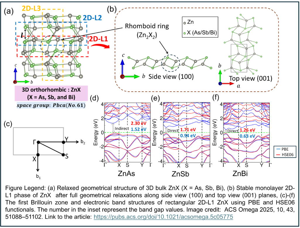
The motivation here goes beyond the general interest in atomically thin semiconductors. The orthorhombic ZnX (X = As, Sb, Bi) compounds contain quasi-layered rhomboid Zn2X2 units embedded in a non-van-der-Waals 3D bulk framework. A bulk crystal without classic layered cleavage does not exclude monolayer design; it simply removes the comfort of obvious exfoliation routes and forces the structural problem back onto bonding topology. In a recent research paper published in ACS Omega, Assistant Professor Dinesh Thapa from Thomas More University working together with Professor Seong-Gon Kim from the Mississippi State University, developed a lattice-engineering framework for deriving and comparing six candidate monolayer structures of ZnAs, ZnSb, and ZnBi extracting from different phases of 3D bulk structures of ZnX using density functional theory (DFT) under periodic boundary conditions. They identified a rectangular 2D-L1 sheet built from relaxed Zn2X2 rhomboid units as the lowest-energy and dynamically stable monolayer across the series at zero strain.
The research team examined six monolayer candidates for each compound: the atomic configurations of three sheets obtained from the orthorhombic bulk and labeled L1, L2, and L3, alongside tetragonal, hexagonal (planar honeycomb), and trigonal (puckered honeycomb) symmetries. The investigators relaxed both atomic positions and lattice vectors for every candidate, and this symmetry design is important because fixing the cell too rigid would have hidden the geometry that the material actually preferred. They found that the bulk-derived L1 sheet relaxed into a rectangular monolayer built around quasi-layered rhomboid Zn2X2 rings, while L2 and L3 also retained rectangular character but did not match L1 energetically. The authors compared the geometrical stability and integrity of those phases by total energy, phonon behavior, exfoliation energetics, mechanical response, and finite-temperature stability, which made the structural claim rest on more than one criterion.
Thapa and Kim also observed that L1 occupied the lowest-energy position across ZnAs, ZnSb, and ZnBi, with the ordering L1 below L3 below L2 and such ranking alone would not have been enough, because metastable sheets often appear competitive before vibrational analysis exposes the problem. They therefore examined phonon dispersions and found that L1 remained free of imaginary modes at zero strain in all three compounds, whereas L2 and the tetragonal phase carried unstable modes, and L3 stayed fully stable only in ZnAs while showing slight soft-mode behavior in ZnSb and ZnBi. Tetragonal geometry came energetically close in ZnSb and even looked favorable in ZnBi, however, that apparent advantage failed to survive the dynamical test. For synthesis, a low static energy is not sufficient if the lattice still prefers to distort. The authors then reinforced the L1 assignment with ab initio molecular dynamics at 300 K and with elastic analysis, arguing that thermal persistence and mechanical admissibility align with the phonon result instead of contradicting it.
The authors examined bulk ZnAs and ZnSb as narrow-gap semiconductors and bulk ZnBi as a semimetal, with the orthorhombic network built from edge-sharing tetrahedra and rhomboid multicenter units. The researchers reported a slightly indirect gap for 2D-L1 ZnAs, but direct gaps for 2D-L1 ZnSb and 2D-L1 ZnBi. L3 remained semiconducting too, though its gap stayed indirect across the series. The investigators also found a more abrupt shift in the tetragonal monolayer, where orbital overlap at the Fermi level produced metallic behavior, thus indicating electronic transition from wide band gap semiconductor to metallic behavior while going from energetically competing 2D-L1 phase to 2D-tetragonal phase. In ZnAs, the team further extracted a negative Poisson ratio for L1, a mechanical response that links the peculiar rhomboid-ring geometry to auxetic behavior. A different local network would not be expected to yield the same coupling between deformation and lateral strain.
Thapa and Kim identified a structural principle for zinc pnictide monolayers: the stable sheet adopts a rectangular lattice inherited from the rhomboid-ring physics of the orthorhombic parent. Many computational searches for new 2D materials begin with familiar structural archetypes, after which chemistry-specific bonding preferences are examined in greater detail but in Thapa and Kim work the bonding chemistry leads to a different structural route. The multicenter bonding character of ZnX pushes the stable monolayer toward a less familiar geometry, and that outcome has consequences well beyond these three compounds. It shows that non-van-der-Waals parents with quasi-layered subunits may still yield viable two-dimensional descendants, but only when the descendant preserves the bonding logic embedded in the bulk.
The authors performed analysis in their paper beyond relaxed structures and band plots to include relative energies, phonons, exfoliation considerations, mechanical checks, thermal trajectories, and hybrid-functional electronic analysis. In the ZnBi case: bulk formation energy remained slightly positive at zero temperature and pressure, but the monolayer question remains open under those conditions. From an applications standpoint, the direct-gap 2D-L1 sheets in ZnSb and ZnBi could become useful where atomically thin semiconductors with larger gaps are needed, especially in optoelectronic settings that do not benefit from metallic leakage. ZnAs is considered interesting for a different reason: a stable auxetic semiconductor is mechanically unusual, and if synthesis catches up, its deformation response could matter in device architectures where strain is not a limitation but part of the operating condition. The new study established a strong theoretical basis, while practical use will depend on experimental validation. Geometry selected by bond topology can control whether a monolayer survives as well as whether it ends up indirect, direct, or metallic. In zinc pnictides, the sheet that the lattice can actually tolerate appears to be the same sheet that produces the most interesting electronic and mechanical outcomes.


Reference
Thapa D, Kim SG. Lattice Engineering Novel 2D Monolayer in Zinc Pnictides. ACS Omega. 2025;10(43):51088-51102. doi: 10.1021/acsomega.5c05775.
Go to ACS Omega