
Significance
Under a finite temperature gradient and electrostatic bias, the transmission probability across a nanometer-scale WSe₂ channel can collapse exponentially within the band gap, forcing charge carriers either to tunnel through a classically forbidden region or to surmount an energy barrier through thermionic emission. That basic transport constraint—set by the spectral profile of τ(E) near the chemical potential becomes especially severe when the channel length extends beyond only a few nanometers. In such a regime, thermoelectric response no longer follows simple metallic intuition, because electrical conductivity, electronic heat flow, and phonon-mediated heat conduction evolve on different physical scales and with different sensitivities to gate voltage and temperature.
Thermoelectric conversion in low-dimensional semiconductors hinges on balancing four interdependent quantities: electrical conductivity, Seebeck coefficient, electronic thermal conductivity, and lattice thermal conductivity. In monolayer transition metal dichalcogenides, sharp features in the density of states near band edges can amplify thermopower but those same spectral features can coincide with suppressed charge transmission. When the chemical potential resides deep inside the band gap, τ(E) approaches extremely small values, which increases |S| through the energy derivative of τ(E), while simultaneously driving the electrical conductance toward zero. The formal structure of ZT makes that tension unavoidable: the numerator scales with S²σ, but both σ and kel depend directly on τ(E), and kph persists even when carriers are frozen out.
Gate-tunable architectures introduce a degree of control that bulk thermoelectrics lack. By shifting the chemical potential relative to the transmission function, one can push a nanojunction from insulating to conducting behavior without altering its atomic composition. In short channels, quantum tunneling dominates midgap transport; in longer channels and at elevated temperatures, thermionic emission over the barrier gains statistical weight. The transition between these mechanisms depends jointly on channel length, temperature, and electrostatic shift. Understanding how that crossover restructures the competition among σ, S, ke, and kph requires a framework that treats electronic and phononic transport on equal footing. This need motivates a first-principles examination of gate-controlled Pt–WSe₂–Pt nanojunctions across channel lengths spanning only a few nanometers, where neither purely quantum nor purely semiclassical reasoning suffices in isolation.
A recent research paper published in ACS Nano and led by Professor Yu-Chang Chen and Yu-Chen Chang from the National Yang Ming Chiao Tung University, the researchers developed a first-principles framework that combines NEGF-DFT electronic transport with nonequilibrium molecular dynamics phonon simulations to evaluate ZT in gate-controlled Pt–WSe₂–Pt nanojunctions. They introduced an effective gate model that shifts the chemical potential differently inside and outside the band gap to capture realistic electrostatic response. They also formulated a quantitative measure of the competition between quantum tunneling and semiclassical thermionic emission, enabling identification of the crossover regime where thermoelectric performance peaks.
The research team constructed Pt–WSe₂–Pt nanojunctions with channel lengths of 3, 6, 9, and 12 nm and optimized their geometries using density functional theory before computing transmission functions through a NEGF-DFT formalism. They extracted τ(E) for each channel length and directly evaluated σ(T, Vg), S(T, Vg), and kel (T, Vg) from the Landauer expressions, while they obtained kph (T) through nonequilibrium molecular dynamics simulations. By assigning a gate efficiency that shifts the chemical potential differently inside and outside the band gap, the investigators translated electrostatic bias into an effective displacement of μ relative to τ(E).
The authors demonstrated that the minimum transmission at the band-gap center decreases exponentially with channel length, which confirms quantum tunneling as the dominant midgap mechanism in short junctions. They observed that for Lch below roughly 9 nm, the minimum conductivity at low temperature tracks that exponential suppression. When they increased the channel length to 12 nm, however, the temperature dependence no longer followed a simple exponential decay, signaling the growing role of thermionic emission. To quantify this shift, the researchers decomposed the conductance into quantum mechanical and semiclassical components and introduced a parameter that measures their relative strength. That construction makes explicit a trade-off: as channel length increases, tunneling weakens rapidly, but thermionic contributions rise only when thermal activation becomes statistically significant.
The study examined how the Seebeck coefficient behaves under these same conditions. The researchers observed that |S| can exceed several thousand microvolts per kelvin when the chemical potential lies near the middle of the band gap, where τ(E) is extremely small but its derivative remains finite. They also showed that ZT remains suppressed in that regime because kph dominates the denominator while σ is negligible. When the gate shifts μ slightly outside the band gap (at the point where τ(E) begins to rise sharply) the system enters a transitional region in which kph and kel become comparable. There, the balance between S²/L and 1 + kph / kel becomes favorable, and ZT reaches its maximum values. The team reported that the 3 nm junction at 500 K achieves ZT above 2, precisely where quantum tunneling and thermionic emission coexist. That coexistence appears less as a coincidence and more as a constraint-driven optimum: only in the crossover does the junction avoid both vanishing conductivity and overwhelming electronic heat conduction.
The findings of Professor Yu-Chang Chen and Yu-Chen Chang refine how thermoelectric optimization should be conceptualized in nanoscale semiconducting junctions. Maximizing the Seebeck coefficient alone misdirects design, since extreme |S| often emerges in regimes where electrical conduction is too weak to support useful power output. On the other hand, pushing the junction fully into a metallic state increases kel through the Wiedemann–Franz relation, which dilutes gains from higher σ. Their analysis showed elegantly that the most effective operating point lies at the edge of the band gap, where transmission rises steeply but has not flattened. In that region, the ratio kph / kel approaches unity, and the denominator of ZT no longer overwhelms S².
Also, the quantum-to-classical crossover plays a structural role in this optimization. In short channels, quantum tunneling preserves conductance even when μ resides near midgap, enabling appreciable S without catastrophic loss of σ. In longer channels, thermionic emission dictates transport, and the optimal gate voltage shifts accordingly. Temperature acts as a second control knob, narrowing the domain where tunneling dominates and expanding the statistical weight of over-barrier carriers. If one were to design adaptive thermoelectric elements integrated into electronic platforms, the combined control of channel length and gate voltage would permit dynamic relocation of the operating point near that crossover. Such adaptability remains bounded by phonon heat flow, which doesn’t diminish as rapidly as electronic contributions in the insulating regime.
To sum up, we believe the work of Professor Yu-Chang Chen and Yu-Chen Chang matters to engineers because it shows that thermoelectric performance in nanoscale devices depends not just on material choice, but on channel length, temperature, and electrostatic control. It demonstrates that maximum efficiency occurs at the crossover between quantum tunneling and thermionic emission. That result changes how engineers should design gate-controlled nanojunctions for energy harvesting or thermal sensing and by tuning the chemical potential near the band-edge transition, devices can achieve higher ZT without sacrificing conductivity. Indeed, Chen and Chang provided a physics-based roadmap for integrating two-dimensional semiconductors into on-chip waste-heat recovery and adaptive thermal management systems.
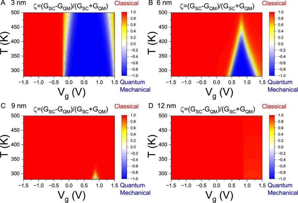
Figure 4. Contour plots depict the quantum-to-classical transition. Contour plots of ζ ≡ (GSC–GQM)/(GSC+GQM) are shown as functions of temperature (250–500 K) and gate voltage Vg (−1.5 to 1.5 V) for Pt–WSe2–Pt thermoelectric junctions with channel lengths Lch= (A) 3 nm, (B) 6 nm, (C) 9 nm, and (D) 12 nm. ζ(T, Vg) represents competitive strength between quantum mechanical (shown in blue) and semiclassical (represented in red) transport mechanisms. Copyright © 2025 The Authors. Published by American Chemical Society. This publication is licensed under CC-BY 4.0 .
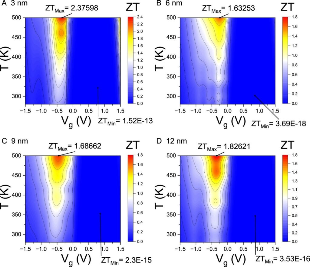
Figure 7. Contour plots of ZT(T, Vg). Contour plots of the thermoelectric figure of merit ZT(T, Vg) are shown over the temperature range of 250–500 K and gate voltage range of −1.5 to 1.5 V for Pt–WSe2–Pt thermoelectric junctions with channel lengths Lch= (A) 3 nm, (B) 6 nm, (C) 9 nm, and (D) 12 nm. The maximum and minimum values of ZT, denoted as ZTMax and ZTMin, respectively, along with their corresponding locations within the T–Vg domain, are also indicated. Copyright © 2025 The Authors. Published by American Chemical Society. This publication is licensed under CC-BY 4.0 .

Reference
Chen YC, Chang YC. Thermoelectric Optimization and Quantum-to-Classical Crossover in Gate-Controlled Two-Dimensional Semiconducting Nanojunctions. ACS Nano. 2025;19(39):34906-34917. doi: 10.1021/acsnano.5c10790.