
Significance
Recently, studies involving the growth of vanadium dioxide films on glass substrates have attracted significant interest amongst various researchers. This is due to its excellent structural phase transition (SPT) and insulator-metal transition (IMT) that can be triggered by an electrical voltage. The optical transmittance of vanadium oxide depends on the changes in the IMT. For instance, insulator-metal transition characteristics enable fast transmission of infrared-light with wavelength larger than 1μm. This has increased the use of vanadium oxide in several optical and thermochromics applications like in the case of intelligent optical windows.
Presently, different methods have been devised to achieve better growth of vanadium dioxide films on glass substrates. Zinc oxide has been used for effective growth of vanadium dioxide films owing to its hexagonal plane orientation. Consequently, transparent conductive Al-doped zinc oxide has effectively controlled infrared-light transmittance. This has led to the fabrication of vanadium dioxide film on Al-doped zinc oxide layer to control optical properties through voltage addition. However, deposition of vanadium dioxide films on Al-doped zinc oxide layer has not been fully explored. The resultant layer enables optical transmittance of infrared light at low voltage.
Recently, a group of researchers at Tokai University: Kenta Sato, Hiroaki Hoshino, Dr. Suruz Mian and Professor Kunio Okimura investigated the growth of vanadium dioxide films on both transparent conductive Al-doped zinc oxide layer /glass and transparent zinc oxide glass substrates. They used both inductively coupled plasma assisted radio frequency magnetron sputtering and conventional radio frequency magnetron sputtering. Also, they determined the advantages of vanadium dioxide deposition at low temperatures. Their work is published in the journal, Thin Solids Films.
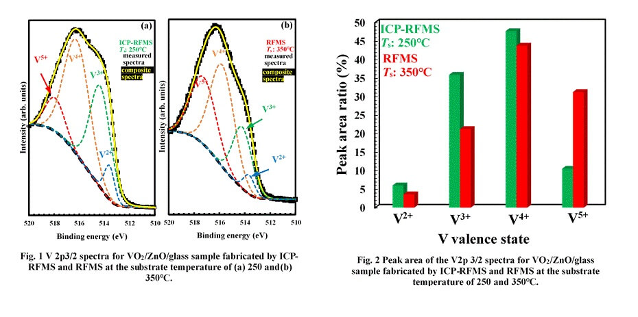
The research team observed that at low temperatures of 250 °C, vanadium dioxide films grown successfully on ZnO/glass substrates due to the introduction of inductively coupled plasma assisted sputtering. Also, the formation of zinc vanadate occurred at the interface region of radio-frequency magnetron sputtering at a temperature of 350°C. Furthermore, a resistivity drop above two magnitude orders was observed in the vanadium dioxide films with the infrared-light transmittance changing from 45-10% in comparison to substrate temperature.
From the scanning electron microscope images and XPS depth results, the authors concluded that the formation of zinc vanadate greatly led to the deterioration of the transmittance of the infrared light. Consequently, the steep interface between the interface of vanadium dioxide and zinc oxide was formed without contaminants compounds. The use of inductively coupled plasma assisted method enabled the growth of vanadium dioxide films on conductive Al-doped zinc oxide at low temperatures.
According to Professor Kunio Okimura and his research team, the simultaneous steep changes in transmittance and resistivity will open new doors for the applications of vanadium dioxide films in different fields including thermochromics devices like smart windows. For instance, the transmittance change observed in vanadium oxide on AZO glass forms the basis of controlling intelligent optical windows electrically.


Reference
Sato, K., Hoshino, H., Mian, M., & Okimura, K. (2018). Low-temperature growth of VO2 films on transparent ZnO/glass and Al-doped ZnO/glass and their optical transition properties. Thin Solid Films, 651, 91-96.
Go To Thin Solid Films