Fabricated via Dry-Etching for Optical and Microelectronic Applications
Significance
Hierarchical structures ranging from microscale to nanoscale sizes are ubiquitous in nature. Although there are numerous building structures, self-assembly provides a more feasible and robust approach for building high-performance hierarchical structures. Self-assembly, especially at the nanoscale level, can be driven by the interactions between chemical functional groups. However, the mechanical engineering strain formed at the interfaces of thin films is crucial for fabricating self-assembled three-dimensional (3D) microarchitectures. Examples include cubes and microcylinders, which have found applications in various fields such as in photonics and electronics.
Similarly, self-assembly by rolling-up of structured thin-film stacks has been extensively investigated. In particular, it has been used to create micromachined devices such as roll-up microtubes with unique three-dimensional geometry desired for various applications. Typically, the fabrication of these microtubular architectures involves using wet-release techniques, which have several drawbacks. It reduces the yield, uniformity and quality of the resulting microtubular architectures as well as the overall deterioration of the device performance. These problems can be attributed to the presence of aggressive reagents and capillary forces.
Dry release methods have been identified as a promising solution due to their ability to delaminate the layer stacks during thermal annealing or when selectively under etched in the gaseous atmosphere. Equipped with this knowledge, a group of researchers at the Institute for Integrative Nanosciences in Germany: Christian Saggau (PhD candidate), Felix Gabler, Dr. Dmitriy Karnaushenko, Dr. Daniil Karnaushenko, Dr. Libo Ma and Professor Oliver Schmidt developed a wafer-fabrication of high quality and high-performance microtubular devices via dry rolling of dielectric, metallic and dielectric/metallic hybrid thin films. The authors purposed to use this method in different microelectronic and optical applications. Their work is currently published in the research journal, Advanced Materials.
In their approach, the process was divided into two: patterning of the thin films in a controlled wafer-scale fashion and dry release of the films in a gas or plasma atmosphere. Self-assembly of prestrained nanomembers was triggered in a controlled manner by etching a thin sacrificial silicon layer on an insulator using dry fluorine chemistry. The potential practical applications of this method in photonics and electronics as well as its complementary metal oxide semiconductor (CMOS) compatibility and integration, were discussed in detail.
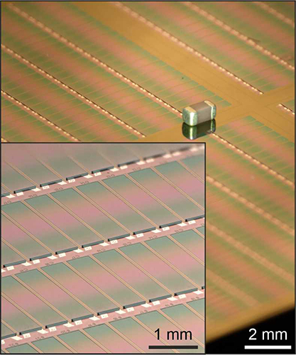
The authors successfully demonstrated a simultaneous self-assembly process of thousands of integrated microcapacitors on a single wafer. The fabrication on a wafer-scale resulted in a high yield of devices with improved performance, uniformity and reproducibility desirable for broad applications in phonics and electronics. For instance, 84% and 91% yield of microcapacitors within the E24 and E12 IEC/EN 60062 industrial standard, respectively. For photonic devices, active microtubular optical cavities were fabricated on a wafer-scale. The optical microtube resonators exhibited optical resonances with a wide spectral range with Q-factors exceeding 7800 which is the highest reported for this kind of optical cavities. Furthermore, it was worth noting that the process quality could be improved in an industrial fabrication line due to its superior optimization deposition and cleanliness.
In a nutshell, a well-controlled and CMOS compatible method for the fabrication of high-quality and high-performance rolled-up microdevices on a wafer-scale is reported. The process addressed the limitations of the conventional wet-etching methods commonly used in the self-assembly techniques and is advantageous because it can be realized using standard tools like those used in the commercial production of photonics and electronic devices. Moreover, the approach can also be applied to other materials used to fabricate electronic and optical devices. In a statement to Advances in Engineering, the authors explained that the guided self-assembly provides opportunities for on-chip large-scale integration of high-performance 3D photonic, electronic and optoelectronic devices.

Reference
Saggau, C., Gabler, F., Karnaushenko, D., Karnaushenko, D., Ma, L., & Schmidt, O. (2020). Wafer‐Scale High‐Quality Microtubular Devices Fabricated via Dry‐Etching for Optical and Microelectronic Applications. Advanced Materials, 32(37), 2003252.
 Advances in Engineering Advances in Engineering features breaking research judged by Advances in Engineering advisory team to be of key importance in the Engineering field. Papers are selected from over 10,000 published each week from most peer reviewed journals.


