Significance Statement
Reversible Insulator-to-Metal Transition (IMT or MIT) phenomenon observed in many transition metal oxides has been attracted much interest from science and industry. Generally, it is occurred under the external stimuli (heat, light, electric field, pressure etc.) at some critical point, inherent for a particular material. A representative canonical IMT material, Vanadium Dioxide (VO2), is “gifted” by the near room temperature transition accompanied by abrupt changes in electrical and optical properties, making this material suitable for various applications, such as switching devices, sensors, memory devices, smart windows etc.
However, until this time, a widespread usage of VO2 was limited by difficulties in its integration with existing silicon-based technology, yielding in poor quality of VO2 and, thus, deteriorated the IMT characteristics. Now, we have overcame the challenges by using a novel buffer layer of aluminum nitride (AlN), placed between a silicon substrate (111) or (001) and the top VO2 thin film. The latter results in epitaxial growth of VO2 having excellent electronic properties with the colossal resistance changes for about four orders of magnitude at the temperature of about 77oC (see Fig.). This research was published in AIP journal of Applied Physics Letters Materials 4,026101 (2016), reference on which is shown below.
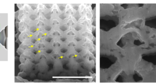
Moreover, in collaboration with the researchers from a MoBRiK company, we went beyond the laboratory samples with a typical size of 2″, and made a Fab line for a consequent and continuous production of the uniform large-area AlN and VO2 films on 8″ Si substrate (Fig.). Based on this, further photolithography fabrication of the Mott IMT devices was established with a number of over 200,000 microsized devices per one 8″ VO2/AlN/Si sample (Fig.). Thus, the developed fabrication line is suitable for a mass production, while the device functionality, due to synergy of VO2, AlN and Si, is able to open a new era in the semiconducting field.


Journal Reference
Tetiana Slusar1, Jin-Cheol Cho1,2, Bong-Jun Kim1, Sun Jin Yun2,3 and Hyun-Tak Kim1,2
[expand title=”Show Affiliations”]- Metal-Insulator-Transition Center, Electronics and Telecommunications Research Institute, Daejeon 305-700, South Korea
- Department of Advanced Device Technology, University of Science and Technology, Daejeon 305-700, South Korea
- Components and Materials Research Laboratory, Electronics and Telecommunications Research Institute, Daejeon 305-700, South Korea [/expand]
Abstract
We report the epitaxial growth and the mechanism of a higher temperature insulator-to-metal-transition (IMT) of vanadium dioxide (VO2) thin films synthesized on aluminum nitride (AlN)/Si (111) substrates by a pulsed-laser-deposition method; the IMT temperature is TIMT ≈ 350 K. X-ray diffractometer and high resolution transmission electron microscope data show that the epitaxial relationship of VO2 and AlN is VO2 (010) ‖ AlN (0001) with VO2 [101] ∥∥ AlN [21̄ 1̄ 0]‖ AlN [21̄1̄0] zone axes, which results in a substrate-induced tensile strain along the in-plane a and c axes of the insulating monoclinic VO2. This strain stabilizes the insulating phase of VO2 and raises TIMT for 10 K higher than TIMT single crystal ≈ 340 K in a bulk VO2 single crystal. Near TIMT, a resistance change of about four orders is observed in a thick film of ∼130 nm. The VO2/AlN/Si heterostructures are promising for the development of integrated IMT-Si technology, including thermal switchers, transistors, and other applications.
Go To APL Mater