Significance
In situ mechanical testing in the transmission electron microscope (TEM) is an important tool to characterize a variety of materials including single-crystals, metallic glasses, thin films, nanowires and even complex materials such as high-entropy alloys. Indeed, TEM has been used extensively for imaging materials at the molecular, granular or sub-granular level, and has helped scientists to understand how these materials behave, because in the electron microscope the electron beam wavelength can probe smaller distances than the visible light microscope. In contrast, another common technique called using scanning electron microscope, the images captured at the sample surface because the electron beam bounces off the surface, while in the transmission electron microscope the electron beam goes through the sample, which must be very thin, and the response is averaged through the thickness. Digital Image Correlation in the SEM has been established and make capturing images easier. However, this has not been done using the TEM, which has much higher magnification capabilities. Full-field measurements at the microscale and nanoscale resulting from in situ TEM experiments would open a new avenue of metrology for materials assessment, especially in regions of high localization such as grain boundaries, crack tips, shear bands in crystals and metallic glasses.
Researchers at University of Illinois Urbana-Champaign led by John Lambros, professor in the Department of Aerospace Engineering and director of the Advanced Materials Testing and Evaluation Laboratory at Illinois. developed a new method to measure changes that occur in materials, such as glasses, at the nanoscale. The research team developed methods for in situ full-field displacement measurement in the TEM. By generating and tracking appropriate speckle patterns on a sample that they can apply DIC and PT on images acquired during in situ loading and deformation experiments. The original research article is now published in Materials Characterization.
The researchers first ion-milled a bend-beam from a bulk piece of silicon dioxide, a type of glass, in the Materials Research Laboratory’s focused ion beam facility. In a vacuum deposition chamber, a thin film of gold is deposited on the beam. Then, the sample is heated and the continuous film breaks up into little islands, which provide sufficient contrast to be visible on the silica sample in the electron microscope.
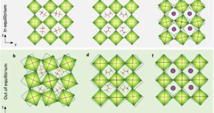
In a nutshell, the new study successfully developed a digital image correlation method in the transmission electron microscope. They confirmed that the method works, now they plan to use the new technique to study the nanoscale behavior of the spinel material.


Reference
Y. Zhang, L. Feng, S. Dillon, J. Lambros, Full-field deformation measurements in the transmission electron microscope using digital image correlation and particle tracking, https://www.sciencedirect.com/science/article/pii/S1044580321007208