Significance
The drive to unlock novel electronic, optical, and structural behaviors has fueled intense global research. Yet, even as the field expands with exciting heterostructures and Janus materials, a deeper frontier—true interlayer hybridization between chemically and electronically dissimilar 2D components—has remained out of reach. New research paper published in Advanced Materials Journal and conducted by Sathvik Ajay Iyengar, Manoj Tripathi, Anchal Srivastava, Abhijit Biswas, Tia Gray, Mauricio Terrones, Alan Dalton, Marcos Pimenta, Robert Vajtai and led by Professor Vincent Meunier and Professor Pulickel M. Ajayan from the Rice University, developed a new “glaphene”—a hybrid material that fuses 2D silica glass and graphene. What distinguishes glaphene is not simply the layering of two materials, but their electronic and structural entanglement at the atomic level. Graphene, celebrated for its semi-metallic conductivity and unparalleled strength, is here juxtaposed with 2D silica glass—a high-bandgap insulator characterized by its amorphous structure and chemical inertness. The two are, by conventional logic, incompatible in both form and function. And yet, this research demonstrates that through an innovative vapor-phase synthesis using a liquid precursor, these disparate entities can be chemically and electronically unified into a metastable, semiconducting material. The current challenges in the field are manifold. While stacking of 2D layers has yielded intriguing van der Waals heterostructures, such constructs often preserve the individual identities of their components, limiting the emergence of genuinely new material behavior. Moreover, Janus materials—where different atoms functionalize each side of a monolayer—remain constrained to particular material classes, predominantly transition metal dichalcogenides. Neither approach typically results in new phases with fundamentally altered band structures or emergent quantum behaviors.
Another longstanding hurdle has been the realization of an “electronic proximity effect” in layered systems—a phenomenon where the electronic states of one layer can significantly influence the other across the interface. Though magnetic proximity effects have been observed, genuine hybridization between insulators and conductors has eluded experimental confirmation, largely due to weak interlayer coupling and insufficient control over lattice mismatch and atomic registries. This is precisely where the current study makes a transformative impact. The researchers sought to not only design but also synthesize and fully characterize a system where these challenges could be overcome. By leveraging a one-pot chemical vapor deposition technique with tetraethyl orthosilicate as the precursor, they managed to grow glaphene films at scale, achieving hybridization verified by atomic-resolution microscopy, spectroscopy, and density functional theory. The result: a new material with an experimentally measured bandgap of ~3.6 eV—positioned between the extremes of its components—and a distinct vibrational and electronic fingerprint attributable to strong out-of-plane pz orbital interactions. The motivation, then, was not simply to create another 2D structure, but to expand the conceptual and synthetic boundaries of what layered materials can be. Glaphene is not just a hybrid—it is a new phase of matter born from the intimate, deliberate entanglement of opposites. This study signals a fundamental shift in how researchers might imagine, build, and utilize 2D materials in the years to come.
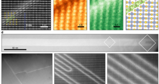
To understand the nature of glaphene—a hybrid born from the unlikely union of 2D silica and graphene—the researchers embarked on a meticulous series of experiments, each step designed to peel back a different layer of this material’s character. Their journey began with synthesis. Rather than stack prefabricated sheets, the team opted for a one-pot vapor-phase growth process using tetraethyl orthosilicate (TEOS) as the single precursor. This choice was deliberate: TEOS decomposes to yield both carbon and silica, allowing for a controlled sequence of graphene formation followed by silica deposition. By fine-tuning the oxygen flow, they managed to navigate a delicate chemical balance—too much, and the graphene would degrade; too little, and the silica layer would fail to form properly. The success of this balancing act became visually clear through electron microscopy, which revealed a coherent, continuous hybrid layer. But forming the structure was only the beginning. To probe whether a true hybridization had occurred—beyond mere stacking—the researchers turned to spectroscopy and mass spectrometry. Time-of-flight secondary ion mass spectrometry (TOF-SIMS) offered a striking clue: the presence of transient SiOCCs₂⁺ fragments at the interface hinted at chemical bonding between silicon and carbon atoms, mediated through oxygen. This interfacial signature faded within less than a nanometer, pointing to a highly localized, structurally unique layer. Simultaneously, x-ray photoelectron spectroscopy (XPS) revealed a co-existence of sp² and sp³ carbon signatures, consistent with out-of-plane bonding characteristic of Si–O–C linkages.
Raman spectroscopy added another piece to the puzzle. Alongside the expected peaks from graphene and silica, the team observed an unexpected vibrational mode near 1050 cm⁻¹—interpreted as a hybridized Si–O–C stretch. Unlike traditional heterostructures, this new mode suggested a physical entanglement of the vibrational dynamics from both materials. Meanwhile, atomic-resolution transmission electron microscopy not only confirmed the presence of both layers but also captured a distinctive moiré pattern—a telltale sign of rotational alignment and lattice strain. That strain, when quantified, revealed minute bond distortions, validating theoretical models of a “disordered crystalline” structure. Finally, perhaps the most profound finding emerged from electronic measurements. Using a combination of ultraviolet photoelectron spectroscopy and reflection electron energy loss spectroscopy, the researchers reconstructed the band structure of glaphene. What they found defied intuition: the hybrid material exhibited a semiconductor-like bandgap of 3.6 eV, a dramatic transformation from its metallic and insulating parents. This shift was driven not by surface effects or external doping, but by genuine electronic proximity—an orbital overlap that bled quantum characteristics from one layer into the other. In that delicate interlayer space, they captured something rare: the creation of a truly new material, one that neither graphene nor silica could be on their own. This study reaches far beyond the mere synthesis of a new material—it opens an entirely different way of thinking about what two-dimensional systems can become when pushed into unfamiliar chemical and electronic territory. At its core, glaphene is not just a novel composite of graphene and 2D silica; it represents a deliberate engineering of interfacial physics, where electronic states from one layer extend into another to forge a new identity. This isn’t stacking—it’s transformation. And that distinction matters.
The significance of this work lies in its successful realization of interlayer hybridization between two chemically dissimilar 2D systems. That’s something the field has long theorized but struggled to demonstrate in practice. While most heterostructures rely on weak van der Waals forces that allow each component to remain largely unchanged, glaphene showcases the power of proximity-driven interactions to completely alter electronic and structural behavior. The emergence of a bandgap that neither graphene nor silica possess individually signals a profound shift—one where the properties of a material are no longer bound by its ingredients alone, but by how those ingredients talk to one another at the atomic scale.
Equally important is the methodology. The researchers didn’t rely on exotic, hard-to-scale fabrication processes. Instead, they achieved hybridization using a single-liquid precursor and a vapor-phase synthesis route—approaches compatible with existing manufacturing technologies. That makes glaphene not just scientifically interesting, but industrially plausible. With this platform, it becomes feasible to think about designing new functional 2D materials from the ground up, using out-of-plane interactions to tailor bandgaps, charge distribution, and optical response in ways that were previously impossible. The implications ripple outward. Glaphene’s moderate bandgap places it in a sweet spot for semiconducting applications like UV photodetectors, photocatalysis, or transparent electronics. More tantalizingly, its moiré-induced strain patterns and hybrid vibrational modes hint at possible uses in neuromorphic devices or quantum information platforms, where controlling exciton behavior and coherence is key. And because the constituent materials—carbon and silica—are both earth-abundant and non-toxic, the pathway to sustainable application is clearer than it is for many current alternatives.


Reference
Sathvik Ajay Iyengar, Manoj Tripathi, Anchal Srivastava, Abhijit Biswas, Tia Gray, Mauricio Terrones, Alan B. Dalton, Marcos A. Pimenta, Robert Vajtai, Vincent Meunier, Pulickel M. Ajayan. Glaphene: A Hybridization of 2D Silica Glass and Graphene. Advanced Materials, 2025; DOI: 10.1002/adma.202419136