Significance
As a result of widespread applications of thin films in optics, optoelectronics and magnetooptics, several methods are used for characterization of thin films, which compute the average thickness da, the thickness non-uniformity Δd, and the complex refractive index of the film, in different spectral regions. The choice of the characterization method of a thin film on a glass substrate specimen, from its normal incidence transmittance spectrum T(λ), depends mainly on whether this spectrum contains interference pattern with several maxima and minima. In the spectral region without interference pattern of T(λ), the film is either strongly absorbing or very thin, and it is most often characterized by the spectroscopic ellipsometry method, which assumes validity of dispersion model for the complex refractive index. In the spectral region with interference pattern of T(λ), scanned by UV-VIS-NIR spectrophotometer, the film can be either dielectric, semiconducting or insulating, with average thickness da ~ [500,5000] nm, and its more accurate characterization is achieved by the envelopes method (EM). The higher accuracy of EM, in comparison with the spectroscopic ellipsometry method, is mainly due to including the interference pattern equation, whereas EM has the additional advantage of not using any dispersion model. However, EM assumes existence of a wide spectral region of quasi-transparency of the film, it contains three subjectively chosen parameters, and employs different algorithms for films with uniform and with non-uniform thickness.
Researchers at Technical University of Sofia, Bulgaria: Assoc. Prof. Dorian Minkov (College of Energetics and Electronics) and Assoc. Prof. George Angelov (Department of Microelectronics), together with Prof. Emilio Marquez from the University of Cadiz in Spain and his Spanish co-workers, proposed optimization of EM (OEM). Their research work is currently published in the journal, Thin Solid Films.
The advantages of OEM compared to EM are: it always results in more accurate characterization of the film, regardless of whether the film has or does not have a wide spectral region of quasi-transparency; optimizes the three subjectively chosen parameters of EM; and employs the same algorithm for uniform and for non-uniform films.
In OEM, the optimization is performed by using original error metrics. Due to inability of EM to separate accurately the absorption from the thickness non-uniformity of the film, this team of researchers used models of four specimens, containing thin films with significantly different absorption and thickness non-uniformity, to investigate the effectiveness of OEM. The OEM characterizations of these model films showed, that the errors in the computations are 0.1% for the average film thickness da, and 0.15% for the refractive index of the film.
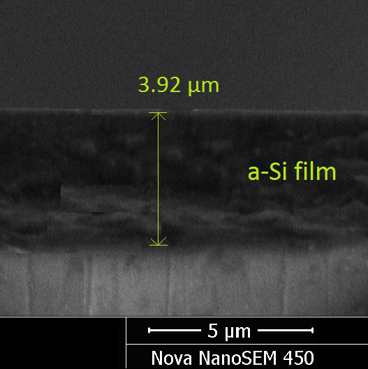
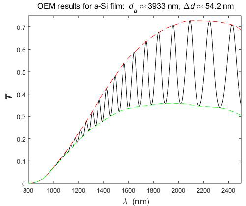
Furthermore, transmittance spectra T(λ) have been scanned and used of two specimens containing a-Si films without wide spectral region of quasi-transparency, and with average film thickness da close to 780 nm and 3920 nm measured by electron microscope. A comparison of these data with film characterizations results showed that the average thickness errors are 38% and 25% for EM characterization, and less than 0.4% for OEM characterization. Achieving such a high accuracy of film characterization by OEM is especially significant for the thicker film, since it seems to be the thickest film ever characterized from its spectrum T(λ).

Reference
Minkov, D., Gavrilov, G., Angelov, G., Moreno, J., Vazquez, C., Ruano, S., & Marquez, E. (2018). Optimization of the envelope method for characterization of optical thin film on substrate specimens from their normal incidence transmittance spectrum. Thin Solid Films, 645, 370-378.
Go To Thin Solid Films