Significance
Ultra-wide-bandgap semiconductors are important in power electronics because they offer a route to switching devices that can withstand large electric fields while sustaining efficient operation under demanding voltage conditions. Within this class of materials, β-Ga2O3 are attracting a lot of attention because of its wide bandgap and high theoretical breakdown field make it a strong candidate for high-voltage power devices, particularly in settings where the material’s field-handling capability can be translated into practical transistor structures. That possibility has motivated sustained work on β-Ga2O3 device design, with both lateral and vertical transistor geometries being explored as researchers try to determine how best to use the material in real high-power operation. The architectural distinction between lateral and vertical devices is not just geometric. Vertical transistors are especially relevant when the objective is to support both high blocking voltage and substantial current transport, since the current path and drift-region design can be arranged in a way that is more naturally suited to that regime. For β-Ga2O3, this has made vertical device development an important scientific and technological goal. Yet the central challenge has been clear for some time: the exceptional material properties of β-Ga2O3 do not automatically produce exceptional vertical transistor performance. To realize high-voltage operation in a vertical structure, the device must incorporate a drift region that is both sufficiently thick and sufficiently lightly doped, while the surrounding structure must also suppress electric-field crowding near the device edge. If any of these conditions is not met, the attainable breakdown voltage falls well below what the material itself would appear to allow.
That difficulty has given the field a very specific unresolved problem. Earlier β-Ga2O3 vertical transistors had already demonstrated kilovolt-class operation, but pushing the breakdown voltage substantially higher required more than incremental processing refinement. It required progress in the epitaxial platform itself. The paper makes this point in direct materials terms. High-voltage vertical transistors need high-quality epitaxial films with donor concentration at or below about 5 × 1015 cm−3 and thickness on the order of at least several tens of micrometers, yet obtaining such films is not straightforward. During halide vapor phase epitaxy, chlorine can be incorporated into β-Ga2O3 and act as a shallow donor, making it difficult to achieve the very low donor concentrations needed for a high-voltage drift layer. At the same time, even with an appropriate drift region, the device still depends on edge-termination measures capable of controlling local electric-field concentration.
In a recent research paper published in Applied Physics Express, Daiki Wakimoto, Dr. Chia-Hung Lin, Dr. Kentaro Ema, Dr. Yuki Ueda, Hironobu Miyamoto, Dr. Kohei Sasaki and Akito Kuramata from Novel Crystal Technology, Inc in Japan, developed a normally-off multi-fin beta-gallium-oxide vertical transistor built on a thick, low-donor-concentration epitaxial layer grown by halide vapor phase epitaxy on a (011) substrate. Its main technical advance is the demonstration of a beta-gallium-oxide vertical transistor that withstands breakdown voltages above ten kilovolts while still preserving normally-off transistor operation, strong current switching, and low specific on-resistance.
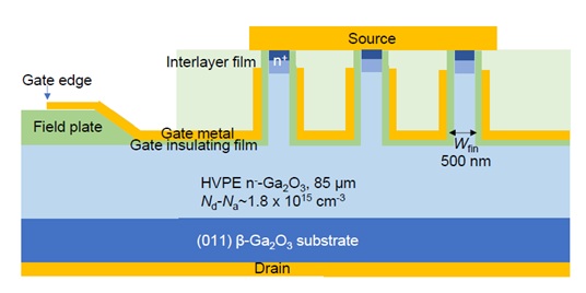
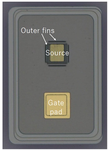
Briefly, the research team fabricated a multi-fin vertical transistor based on beta-gallium oxide using a thick, lightly doped epitaxial layer grown by halide vapor phase epitaxy on a beta-gallium-oxide substrate with the crystallographic orientation chosen to support low donor incorporation. The fabrication sequence established the channel-access and contact structure through silicon implantation, annealing, dielectric formation, dry etching of the fins, planarization, gate formation, and final source and drain metallization. What matters scientifically is not the fabrication sequence alone, but how the device structure was designed to produce the intended electrical behavior: a thick, lightly doped drift region for high-voltage blocking, combined with a fin-based vertical channel and a field-plate-assisted gate arrangement that supports normally-off operation. The authors designed the multi-fin layout with clear attention to geometric control and device uniformity. The active fins were placed within an outer fin arrangement so that the operating channels would behave as consistently as possible and so that variations introduced during dry etching would be reduced. That choice matters because more uniform fin geometry leads to cleaner and more reproducible transistor behavior rather than performance shaped by local structural irregularities. The source electrode was also deliberately pulled back from the fin edge to avoid unintended gate-source contact in regions where etching could distort the fin profile. Electrical measurements showed that the device operated in a normally-off mode. The threshold behavior, strong current modulation, and steep subthreshold response all point to effective control of the channel by the gate. These characteristics are important when considered together, because they show that the fin-channel design and gate-stack integration did not sacrifice switching behavior in the effort to reach high blocking capability. The reported hysteresis remained modest, and the gate current stayed below the measurement limit under the tested conditions, which supports the view that the gate operation was well controlled.
The output characteristics are important for the same reason and the device can block high voltage and also maintains useful conduction performance in the on-state. The authors evaluated the current flow using an effective conductive area that accounts for current spreading in the drift region rather than relying only on the lithographic top-surface geometry. Within that interpretation, the transistor combined solid current conduction with very high off-state blocking capability.
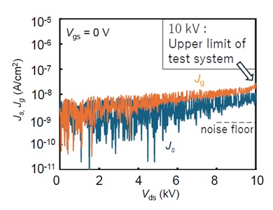
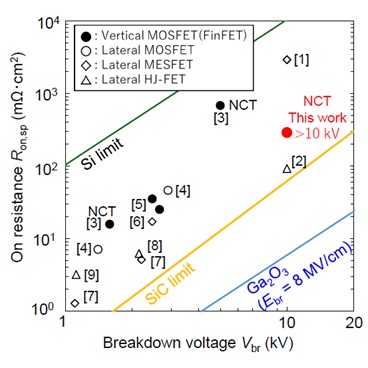
To prevent premature breakdown through air, the measurements were carried out in an insulating liquid, and the device sustained a breakdown voltage above ten kilovolts. In fact, the measurement was limited by the voltage range of the test system rather than by a confirmed breakdown of the device below that level. The estimated electric field in the trench region was correspondingly very high. The authors state that this is the highest breakdown voltage ever reported for a beta-gallium-oxide vertical transistor, exceeding the previous best result for this device class by more than a factor of two. They also report a strong power figure of merit, reinforcing that this was not a single-metric gain but a meaningful advance in vertical beta-gallium-oxide transistor performance. The authors’ work demonstrated what kind of material-device integration is required for β-Ga2O3 vertical transistors to enter a much higher breakdown-voltage regime. The logic is visible throughout the paper: low donor concentration in a thick epitaxial drift layer, achieved on a (011) substrate where Cl incorporation is suppressed, is paired with a multi-fin normally-off structure and field management at the device edge. The breakdown performance is therefore not an isolated metric but the outcome of a coherent design direction grounded in how the electric field is distributed in the device. There is also a meaningful balance here between voltage blocking and transistor operation. In Daiki Wakimoto and colleagues work, the device still shows threshold control, a large on/off ratio, low measured gate current, and a specific on-resistance that keeps the conduction side of the story in view. Its contribution is more disciplined than that. It shows that a normally-off β-Ga2O3 vertical transistor can be pushed past 10 kV while retaining a credible switching profile and a measurable power figure of merit. Earlier β-Ga2O3 vertical transistors had already shown that kilovolt-class blocking was possible and the new device reported by the authors moves the conversation into a distinctly higher-voltage category and narrows the gap between what the material suggests in principle and what a vertical transistor has actually demonstrated in practice. Just as important, the result reinforces the value of the (011) orientation for HVPE-grown low-doped epitaxial layers when the target is vertical high-voltage operation. The paper’s final implication remains measured: it points to the strong potential of Ga2O3 vertical power devices.
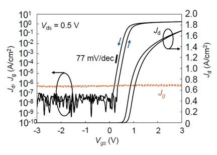
along with the extracted subthreshold slope.
[1] H. Liu et al., IEEE Electron Device Lett. 44, 1048 (2023).
[2] Y. Qin et al., IEDM2024.
[3] D. Wakimoto et al., IWGO2022.
[4] Y. Lvet al., IEEE Electron Device Lett. 41, 537 (2020).
[5] W. Li et al.,IEEE IEDM Tech. Dig., p. 270 (2019).
[6] A. Bhattacharyyaet al.,IEEE Electron Device Lett.42, 1272 (2021).
[7] A. Bhattacharyyaet al., IEEE Electron Device Lett. 43, 1637 (2022).
[8] C. Wang et al.,Appl. Phys. Lett.120, 112101 (2022).
[9] S. Roy et al., IEEE Electron Device Lett.42,1140 (2021).

Reference
Wakimoto, Daiki & Lin, Chia-Hung & Ema, Kentaro & Ueda, Yuki & Miyamoto, Hironobu & Sasaki, Kohei & Kuramata, Akito. (2025). A multi-fin normally-off β-Ga2O3 vertical transistor with a breakdown voltage exceeding 10 kV. Applied Physics Express. 18. 10.35848/1882-0786/ae0d2a.
Go to Journal of Applied Physics Express