Significance Statement
Thermoelectric materials can serve as an alternative potential source of power by the simple use of the interconvert gradients in electric potential and temperature. Its performance given by the dimensionless figure of merit ZT depends on the Seebeck coefficient, electrical resistivity, thermal conductivity and absolute temperature.
When determining the Seebeck coefficients, different configurations of 2-probe or 4-probe have been used. The hot-strip method used for thin films measurement usually employs 2-probe geometry in an axial flow arrangement. However, they face complexity from point of sample preparation, non-effective consideration of electron-transport through the supporting membrane and also generates anisotropic voltage signals across the normal to hot-cold junction line when films deposition on real materials is considered.
The pseudo-binary alloys of (GeTe)m-(Sb2Te3)n have been used in data storage for couple of years because of their ultrafast phase switching between metastable crystalline and amorphous phases. However, despite theoretical works on different compositions of GeSbTe alloy films, experimental reports on thin films are still in starting phase and a proper exploration of its potential is needed for industrial applications.
A collaborative research team of Dr. Manish Kumar, Mr. Athorn Vora-ud and Professor Jeon Geon Han from Center for Advanced Plasma Surface Technology at Sungkyunkwan University (Republic of Korea) and Dr. Tosawat Seetawanb from Sakon Nakhon Rajabhat University (Thailand) performed this work. Dr. Kumar developed the facile thin films thermoelectric measurement system to be used in the temperature range of 300K to 600K. Mr. Vora-ud deposited the films and all authors contributed in analysis of the results. The work published in journal, Materials and Design uses the same system to investigate the thermoelectric properties of Ge2Sb2Te5 thin films synthesized by pulsed DC magnetron sputtering method.
In their study, the researchers used a variety of techniques in their experiments such as an optical emission microscopy to perform plasma diagnostic. Thickness of the deposited film was measured using surface profiler to evaluate the film growth rate. The author also made use of x-ray diffraction technique and field emission scanning electron microscopy for phase identification and surface morphology coupled with atomic composition of Ge2Sb2Te5 thin films respectively. Electrical properties of as-deposited thin films were measured by a two-probe method and annealed films by a four-point probe of the van der Pauw method using a Hall measurement system.
Seebeck coefficients were measured using the authors developed measurement set-up which consists of two copper blocks (for hot and cold junction) and a 6-probe arrangement mounted on an aluminum base plate with the support of aluminum shafts.
The researchers found that intensities of emission lines of germanium, antimony and tellurium slightly enhanced when increasing the working pressure which is an indication of plasma density enhancement but their intensity excitations were relatively weak in comparison of argon excitations. Beyond 6mTorr, the discharge power remained more or less similar up to 8mTorr and deposition increased linearly from 400nm/min to 440nm/min which confirmed enhancement of plasma density with increasing working pressure.
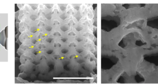
It is worthy to mention that all films were deposited with high uniformity and compactness without any signature of surface defects. As-deposited films have surface features which correspond to amorphous nature after annealing.
Resistivity value decreased from 1.55Ωcm (as-deposited) to 4.76 x 10⁻²Ωcm (annealed at 673K). Resistivity also decreased on increasing thickness of films (from 25nm to 200nm) while there was an increase in resistivity with increase of working pressure from 5mTorr to 8mTorr.
Seebeck coefficient for fixed thickness 200nm and working pressure of 6mTorr was highest at 271.50μV/K at annealing temperature of 473K. From the results also, appropriate resistivity needs optimum thickness equal to 200nm for good value of power factor and optimum pressure condition of 6mTorr is suggested.
It can be concluded from the authors findings that the throughout process greater than 400nm/min and obtained Seebeck coefficient value of 271.50μV/K are highly promising for industrial utilization. According to Dr. Kumar “This is the first step in development of low cost thermoelectic measurement systems ready for commercialization”.


Journal Reference
Manish Kumar1 , Athorn Vora-ud1,2, Tosawat Seetawan2, Jeon Geon Han1 . Study of pulsed-DC sputtering induced Ge2Sb2Te5 thin films using facile thermoelectric measurement, Materials & Design, Volume 98, 2016, Pages 254–261.
[expand title=”Show Affiliations”]- Center for Advanced Plasma Surface Technology, NU-SKKU Joint Institute for Plasma-Nano Materials, School of Advanced Materials Science and Engineering, Sungkyunkwan University, Suwon 440-746, Republic of Korea
- Program of Physics, Faculty of Science and Technology, Sakon Nakhon Rajabhat University, Sakon Nakhon 47000, Thailand
Go To Materials & Design