Significance
Graphene is a single layer of carbon atoms arranged in a two-dimensional honeycomb lattice with extraordinary electrical, thermal, and mechanical properties which make it an ideal candidate for a wide range of applications, including next-generation electronics, photonics, and quantum metrology. One promising method for producing high-quality graphene uses direct epitaxial growth on semi-insulating silicon carbide (SiC). This approach leverages the compatible crystallographic structures and complementary physicochemical properties between epitaxial graphene (EG) and SiC and offers a streamlined route that eliminates the need for transfer during device processing. Despite its potential, the epitaxial growth of graphene on SiC has some limitations related to the quality and cost of production. Traditional annealing methods require temperatures above 1000°C with prolonged heating and cooling cycles which increase production costs and harder to achieve consistent high-quality graphene layers
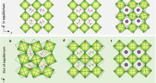
To this account, new study published in Journal of Advanced Functional Materials and conducted by Dr. Ye-Chuang Han, Shi-Hao Yin, Jun-Rong Zheng, Yuan-Fei Hu, Li Sun, Professor Li Zhang, Professor Zhong-Qun Tian, and led by Professor Jun Yi from the Department of Electronic Engineering at Xiamen University developed a novel thermal shock annealing (TSA) method for the epitaxial growth of graphene on SiC which significantly reduce the annealing time while improving the quality and cost-effectiveness of the graphene produced. The researchers initiated their experimental work by synthesizing SiC@EG nanoparticles (NPs) using a TSA method. They used industrially mass-produced β-SiC powder as the precursor. The bulk SiC powder was initially broken into finer powder with an average size of 102 nm through laser fragmentation in liquids and the process involved laser irradiation of SiC suspensions, which facilitated the breakdown of larger particles into nanoscale sizes. Subsequently, the fragmented SiC powder underwent a calcination and etching process to remove carbon or superficial silica residues which ensured a clean surface for epitaxial graphene growth. They applied the new TSA method to grow epitaxial graphene on the prepared SiC NPs under ambient pressure of argon. The high-temperature pulse provided by TSA enabled the rapid and controlled growth of graphene within 10 seconds. The approach resulted in SiC@EG powder with an average size of 113 nm and demonstrated a slight increase in particle size due to the transient high-temperature pulse. The TSA method proved to be highly efficient, producing SiC@EG NPs that exhibited mono- or bi-layer graphene with negligible structural defects. The authors wanted to optimize the TSA process so they studied the influence of temperature and annealing time on the quality of the epitaxial graphene. They analyzed the defect density (ID/IG) and layer number (I2D/IG) of the graphene and found higher temperatures facilitated the reduction of defects and the formation of fewer graphene layers with an optimal temperature of 1800°C was identified for achieving high-quality graphene with minimal structural defects. Additionally, the researchers found that when annealing time extended from 3 to 10 seconds at this temperature did not significantly improve the quality but did result in an increase in the number of graphene layers. The results from the transmission electron microscopy images confirmed the presence of monolayer graphene on SiC NPs after thermal treatment at 1800°C for 5 seconds under 1 atm of argon. In contrast, 4 to 5 layers of graphene were observed when the same temperature was applied for 5 seconds under a low-pressure environment. This finding underscored the importance of maintaining an optimal pressure to control the growth rate and quality of the graphene layers. The researchers also investigated the sintering behavior of SiC NPs during the TSA process. Brunauer-Emmett-Teller (BET) surface area analysis revealed that prolonged exposure to elevated temperatures led to significant sintering of SiC NPs. For instance, there was a 7.1% and 10.7% decrease in BET surface area after 5 and 10 seconds of TSA treatment, respectively. The results indicated that the seconds-scale duration of TSA was crucial for kinetically constraining the sintering of SiC NPs, whereas traditional annealing methods, which require minutes to hours, resulted in severe and irreversible sintering. Moreover, the TSA method effectively mitigated the step bunching conundrum, a common issue in conventional high-temperature annealing. Atomic force microscopy (AFM) characterization showed that the surface roughness of epitaxial graphene grown on SiC wafers using TSA was significantly reduced compared to furnace-grown samples. Specifically, the roughness of the EG/SiC wafer prepared by TSA was only 1/8 of that observed in samples grown by traditional furnace annealing. This improvement in flatness is critical for enhancing the electrical conductivity and overall performance of the graphene. To demonstrate the scalability of the TSA method, the researchers applied it to grow epitaxial graphene on centimeter-scale α-SiC wafers. The process parameters were identical to those used for SiC NPs, with the SiC wafer clamped on two layers of carbon paper and subjected to TSA at 1800°C for 5 seconds under an argon atmosphere. Raman spectroscopy and AFM characterization confirmed that the graphene grown on SiC wafers exhibited high quality, with fewer structural defects and improved flatness compared to samples produced by conventional methods. They found that the TSA-grown EG/SiC samples displayed a low sheet resistance of 0.19 Ω/sq, remarkably lower than that of multilayer or defect-rich EG/SiC counterparts. To demonstrate the ability to produce high-quality graphene using TSA, the researchers explored its application in surface-enhanced infrared absorption (SEIRA). They assembled a monolayer of p-nitrobenzenethiol (p-NTP) on a gold film and dispersed SiC@EG NPs on the surface. According to the authors, the SEIRA tests showed that SiC@EG NPs significantly enhanced the detection sensitivity of p-NTP and achieved detection at the monolayer level. Additionally, the SiC@EG NPs exhibited exceptional chemical stability, maintaining high sensitivity after 10 hours of immersion in acidic and alkaline solutions. Electromagnetic simulations using the finite element method indicated that graphene plasmon resonance on SiC@EG NPs led to a three-orders-of-magnitude enhancement in the infrared signal. The simulations also showed that varying the diameter of SiC@EG particles allowed for broadband infrared signal enhancement, further demonstrating the versatility and effectiveness of the TSA-grown graphene for SEIRA applications.
In conclusion, the new study led by Professor Jun Yi and his team at Xiamen University developed and validated TSA method for the direct epitaxial growth of graphene on semi-insulating SiC. The TSA method enables the rapid production of high-quality, few-layer graphene with minimal structural defects. This is achieved through precise control of temperature and annealing time, ensuring the graphene layers are uniformly grown on the SiC substrate. Traditional annealing methods are time-consuming and expensive, requiring prolonged heating and cooling cycles. In contrast, the TSA method significantly reduces the annealing time to just a few seconds, thereby cutting down on energy consumption and overall production costs. This efficiency makes the method highly attractive for industrial-scale graphene production. Moreover, the TSA method results in a scalable, versatile, smoother, flatter graphene layer with enhanced electrical conductivity. There are significant implications for using the new method, for instance, the high-quality graphene produced via the TSA method can be used in next-generation electronic devices, including transistors, sensors, and flexible electronics. Additionally, the precise control over graphene layer thickness and quality afforded by the TSA method can enhance applications in quantum metrology, where graphene’s exceptional electronic properties can be used for high-precision measurements as well as chemical sensing and spectroscopy.


Reference
Y.-C. Han, S.-H. Yin, J.-R. Zheng, Y.-F. Hu, L. Sun, L. Zhang, Z.-Q. Tian, J. Yi,* Epitaxial Growth of Graphene on SiC by Thermal Shock Annealing Within Seconds. Adv. Funct. Mater. 2024, 34, 2307298. https://doi.org/10.1002/adfm.202307298