Significance
The discovery of semiconductors more than half a century ago has revolutionized the world of technology. Transistors and integrated circuits form the basis upon which our computers and smart gadgets are built. Unlike more than fifty years ago when computers required large spaces, today their sizes have been reduced significantly due to the emergence of more advanced methods for fabricating transistors and integrated circuits.
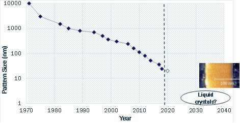
Professor Albert Schenning and Koen Nickmans (PhD student) from the Eindhoven University of Technology contributed a comprehensive review and their expert opinions on patterning technologies for fabrication of more advanced integrated circuits, ranging from the traditional photolithography up to the currently used extreme U-V lithography among other techniques. Their main focus was on performing nanopatterning at sub- 5 nm scale for the next generation’s lithography. Their review is published in Advanced Materials.
Extreme-UV lithography has been recently employed for the production of smaller features. It utilizes radiation of wavelength 13.5 nm. Considering its complex and expensive nature the effectiveness in the manufacturing of the next generations integrated circuits, flash disks, and other electronic devices has been questioned. The alternative top-down nanofabrication techniques are also limited. For example, , electron beam lithography is considered to be slow and expensive, and nanoimprint technology which directly replicates features onto a surface by stamp process faces problems due to improper alignment and contamination.
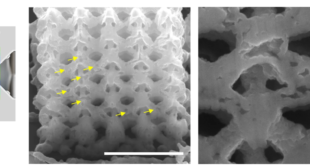
As an alternative to the above top-down methods, bottom-up nanopatterning involving the directed self-assembly (DSA) of block copolymers (BCPs) has been widely accepted. The formation of the nanostructure arrays is due to the microphase separation of the incompatible blocks under the guidance of the top-down process. A significant improvement of DSA is that it allows the generation of circuit elements by self-assembling the nanostructure across the wafer, followed by pattern transfer through the application of wet and dry processinges. Despite the effectiveness of the DSA process, typical feature sizes are still limited to approximately 10 nm, and the large-scale alignment of features necessary for integratione with microelectronics fabrication processes is a challenge
A potential solution to the problem is to use liquid crystalline molecular building blocks as patterning materials. These self-assembled molecular systemsmaterials are capable of achieving even smaller dimension as compared to the BCP method. As a result, they can effectively achieve nanopatterning at 5 nm scale as it employs the use of more efficient lithographic templates resulting from high-order liquid crystals. They also exhibit better properties such as high order, and low viscosity which enables their self-assembly and, proper alignment at smaller length scales compared to BCP DSA processes. This has also seen the increasing use of liquid crystal molecules as building block for functional nanostructured materials.
According to Schenning and Nickmans, sub-5 nm nanopatterning using liquid crystals will help advance the future of nanotechnology, especially nanopatterning for the creation of more advanced devices. However, this will only be realized after addressing some of the challenges associated with the integration of these materials with the existing nanopatterning technologies. The challenges include the use of appropriate metrology tools, suitable pattern transfer methods, the mechanical stability of the features among others.


References
Koen Nickmans, Jeffrey N. Murphy, Bas de Waal, Philippe Leclère, Jan Doise, Roel Gronheid, Dick J. Broer, Albert P. H. J. Schenning. Sub-5 nm Patterning by Directed Self-Assembly of Oligo(Dimethylsiloxane) Liquid Crystal Thin Films. Adv. Mater. 2016, 28, 10068–10072.
Koen Nickmans, Gerardus M. Bögels, Carlos Sánchez‐Somolinos, Jeffrey N. Murphy, Philippe Leclère, Ilja K. Voets, Albert P. H. J. Schenning. 3D Orientational Control in Self‐Assembled Thin Films with Sub‐5 nm Features by Light. Small, 2017, 13, 1701043.
Koen Nickmans, & Albert P.H.J. Schenning, Directed Self-Assembly of Liquid-Crystalline Molecular Building Blocks for Sub-5 nm Nanopatterning. Adv. Mater. 2018, 30, 1703713
Go To Advanced Materials