Significance
GaN-based light-emitting diodes (LEDs) are widely used for lighting and display technologies, but they come with a notable drawback. The p-type GaN material used in these LEDs has poor conductivity due to the difficulty of heavy doping, which means the current does not spread efficiently across the surface. As a result, the performance of the LEDs is limited, and transparent electrodes have become a necessary solution to ensure current spreads evenly across the device. For years, indium tin oxide (ITO) has been the go-to material for transparent electrodes because of its relatively low electrical resistance and decent transparency. However, ITO is far from perfect. Its transparency drops off dramatically in the ultraviolet (UV) spectrum which makes it less effective for UV-based LEDs. On top of that, ITO is brittle, so it is difficult to be used in flexible devices and it relies on indium a really rare and expensive material. These shortcomings have driven researchers to look for better alternatives. That is where graphene comes into the picture because It offers superior transparency in the UV range, unmatched mechanical flexibility, and a more sustainable alternative to ITO. However, despite all of graphene’s potential, there are still significant challenges to using it in real-world devices. One of the main issues lies in the transfer process. Typically, graphene is grown on metal surfaces using a method called chemical vapor deposition, but it then has to be transferred to the target surface. Unfortunately, this process is far from perfect—it often damages the graphene, introduces contamination, and leads to misalignment, all of which reduce its quality and performance. Additionally, traditional patterning methods such as photolithography can further harm the graphene and complicate the manufacturing process.
To address these long-standing challenges, a team of researchers led by Penghao Tang, Yu Mei, Zaifa Du, Aoqi Fang, Fangzhu Xiong, and Professor Weiling Guo from Beijing University of Technology, alongside Professor Jie Sun from Fuzhou University, developed an innovative transfer-free patterning technique for graphene. Their findings, published in the Journal of Materials Chemistry C, offer a new solution for fabricating graphene transparent electrodes, specifically for near-ultraviolet GaN-based LEDs. Their approach uses nickel (Ni) as both a growth catalyst and an etching mask which allows graphene to grow directly in a patterned form without any post-growth transfer steps. To prevent damage to the GaN substrate during high-temperature graphene growth, the researchers introduced a thin layer of silicon dioxide (SiO₂) as an isolation barrier. This layer effectively protects the substrate, avoiding unwanted chemical reactions and thermal damage, which are common problems in traditional methods.
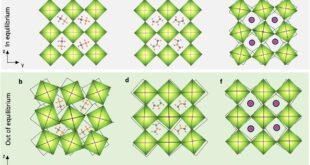
The researchers began by depositing a thin layer of Ni onto the GaN substrate. Nickel served two important roles: it acted as both the etching mask and the catalyst for graphene growth. However, there was a catch—at the high temperatures required for graphene growth, Ni and GaN could interact in ways that would damage both the substrate and the graphene. To solve this, the authors added a thin SiO₂ layer between the two. This SiO₂ barrier worked like a protective shield, preventing any unwanted reactions and ensuring that the Ni could do its job at 650°C without a hitch. Once the Ni was patterned, it guided the growth of graphene directly onto the surface using plasma-enhanced chemical vapor deposition. This step alone was a big deal because it completely eliminated the need for transferring graphene, which is often messy and damaging. After the graphene was successfully grown, the team introduced a clever process called penetration etching. Here, they spin-coated a stabilizing layer of polymethyl methacrylate (PMMA) on top of the graphene. This coating allowed them to carefully etch away both the Ni catalyst and the SiO₂ layer without disturbing the patterned graphene beneath. The PMMA-supported graphene then “fell” neatly onto the GaN surface, creating a clean, direct contact.
Next came the real test: seeing how the graphene electrodes performed. The research team compared three types of LEDs—those with graphene electrodes that used the SiO₂ isolation layer, those without the layer, and conventional ITO-based LEDs. The results were clear. While ITO LEDs had slightly better electrical performance due to lower resistance, graphene LEDs stood out in optical performance, particularly in the ultraviolet range. At 398 nm, the graphene’s transmittance remained exceptionally high, unlike ITO, which dropped sharply. This led to graphene LEDs emitting brighter, more uniform light, with radiant flux measurements confirming their advantage. The SiO₂ layer’s importance became even clearer when the team examined LEDs made without it. In those devices, defects abounded. SEM imaging revealed pits and voids on the GaN surface, caused by Ga atoms diffusing into the Ni at high temperatures. These defects disrupted the graphene’s structure and reduced its transmittance which resulted in weak, uneven light output. To tie it all together, the researchers used atomic force microscopy to analyze the surface. The results aligned perfectly with the SEM findings—samples with the SiO₂ layer had smooth, undamaged GaN surfaces, while those without it showed significant roughness and degradation.
In conclusion, Professor Weiling Guo and colleagues successfully presented an innovative graphene technology by developing a transfer-free patterning method which make it much easier to produce high-quality graphene electrodes for near-ultraviolet GaN-based LEDs. The results are just as impressive as the method itself. The study highlights graphene’s superior optical properties, especially in the ultraviolet range. While ITO—the material most commonly used for transparent electrodes—loses its transparency in the UV spectrum, graphene maintains excellent clarity. This makes graphene an ideal choice for UV-LED applications. In fact, the researchers showed that LEDs using graphene electrodes achieved better light output (radiant flux) at 398 nm compared to their ITO-based counterparts. This proves that graphene is not just a worthy alternative but a superior solution for applications that demand high UV transparency, such as UV sterilization tools, medical imaging systems, and advanced display technologies. We believe the impact of this study does not stop at UV-LEDs and the transfer-free graphene fabrication method can indeed open doors to a wide range of future technologies, including flexible electronics, transparent touchscreens, and next-generation solar cells. Its simple, scalable nature makes it highly appealing for industrial use.


Reference
Tang, P., Sun, J., Mei, Y., Du, Z., Fang, A., Xiong, F., & Guo, W. (2024). A Patterning Technology of Transfer-Free Graphene for Transparent Electrodes of Near-Ultraviolet Light-Emitting Diodes. Journal of Materials Chemistry C. , 12, 9824