Significance
The study of thermal and electronic transport in nanoscale systems is essential to advancing modern technology, especially as electronic devices shrink to unprecedented dimensions and copper, a cornerstone material in electronic interconnects due to its exceptional electrical and thermal conductivity, faces significant performance challenges at these reduced scales. As metallic films and structures approach dimensions comparable to the mean free path of electrons, scattering mechanisms such as boundary scattering and grain boundary effects dramatically influence thermal and electronic behavior. Understanding these phenomena is crucial for designing reliable and efficient components in advanced semiconductor technologies. One of the fundamental challenges lies in predicting how various scattering mechanisms interact and contribute to the overall resistance of a system. Matthiessen’s rule, a widely accepted principle, suggests that scattering rates from different mechanisms—such as electron-phonon interactions and boundary scattering—add linearly and independently. While this rule provides a simplified framework for analyzing transport properties, its validity at nanoscale dimensions and typical operational temperatures has remained uncertain. Previous studies have suggested that deviations from this rule might occur due to the interplay between scattering processes, particularly as films become thinner or exhibit structural complexities such as grain boundary segregation. In addition to these theoretical concerns, there are pressing practical challenges in the realm of integrated circuit design. As devices become smaller, the reliability of their interconnects is increasingly dictated by the ability to maintain thermal and electrical performance under stringent conditions. Failures in accurately modeling and predicting transport properties can lead to overheating, energy inefficiencies, and reduced device lifespans. These challenges underscore the urgent need for a deeper understanding of the mechanisms governing thermal and electronic transport in thin films.
To this note, recent research paper published in Nature Communications and conducted by Md. Rafiqul Islam, Pravin Karna, John Tomko, Eric Hoglund, Daniel Hirt, Md Shafkat Bin Hoque, Saman Zare, Kiumars Aryana, Thomas Pfeifer, Christopher Jezewski, Ashutosh Giri, and led by Professor Patrick Hopkins from the University of Virginia, together with Colin Landon, Sean King and Christopher Jezewski from Intel Corporation evaluated Matthiessen’s rule in copper thin films across a range of thicknesses, microstructures, and processing conditions. Using innovative techniques such as steady-state thermoreflectance and infrared ellipsometry, combined with advanced computational methods, the researchers aimed to disentangle the contributions of different scattering processes. The overarching goal was to provide experimental validation of Matthiessen’s rule at room temperature, a condition highly relevant for real-world applications.
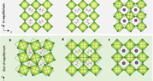
The researchers examined films with thicknesses ranging from 27 nanometers to 5 micrometers, they explored the interplay of boundary scattering, grain size, and grain boundary segregation under conditions relevant to modern electronic devices. These films were synthesized using physical vapor deposition (PVD) and electroplating (EP) methods, ensuring a diverse range of microstructures for analysis. The films were also subjected to annealing at varying temperatures to assess the effects of grain coarsening and chemical changes on their properties. One of the key techniques employed was steady-state thermoreflectance (SSTR), which enabled precise measurements of in-plane thermal conductivity. The results revealed a significant reduction in thermal conductivity as film thicknesses dropped below the electron mean free path of copper, approximately 39 nanometers. This reduction was attributed to increased electron-boundary scattering, a phenomenon expected in nanoscale systems. In thicker films, where the grain size and thickness exceeded the electron mean free path, thermal conductivity values approached those of bulk copper, reaffirming the dominance of intrinsic electron-phonon interactions in these cases. To further understand the role of electron scattering, the team utilized infrared variable angle spectroscopic ellipsometry (IR-VASE). This approach allowed them to quantify electron scattering rates by analyzing the optical properties of the films. The findings showed that as the film thickness decreased, electron relaxation times shortened, corresponding to higher scattering rates. These results aligned with the thermal conductivity trends observed in the SSTR measurements, providing robust evidence of boundary scattering effects. Annealing experiments added another layer of complexity to the study. While annealing generally led to grain coarsening, particularly in thicker films, the thinnest films exhibited a unique behavior. For 27-nanometer films, tantalum (Ta) diffusion into grain boundaries during annealing created TaOx complexes, which acted as additional scattering centers. This segregation process introduced further reductions in thermal conductivity, distinct from those caused by boundary scattering alone. These observations highlighted how chemical interactions at the grain boundaries could influence heat transport in nanoscale films.
The authors also probed electron-phonon interactions using a sub-picosecond pump-probe thermoreflectance technique. They discovered that the electron-phonon coupling factor remained constant across all film thicknesses and microstructures, even in the presence of grain boundary segregation. This consistency provided strong experimental support for Matthiessen’s rule, which posits that electron-phonon scattering occurs independently of other scattering processes, such as boundary or segregation effects.
In conclusion, the study by Professor Patrick Hopkins and colleagues holds profound significance for both fundamental physics and technological applications, particularly in the fields of nanotechnology and semiconductor design. By experimentally validating Matthiessen’s rule in nanoscale copper films, the research bridges a crucial gap between theoretical assumptions and real-world behavior. It establishes that electron-phonon scattering remains independent of boundary and grain boundary segregation effects, even as film dimensions shrink below the electron mean free path. This finding is a cornerstone for understanding thermal and electronic transport in metals, as it simplifies the complex interplay of scattering mechanisms into predictable, additive contributions. On a practical level, the insights gained have transformative implications for the semiconductor industry. As integrated circuits become increasingly miniaturized, reliable interconnects are essential for maintaining performance and thermal stability. The study’s confirmation that boundary scattering dominates conductivity reductions at reduced dimensions allows engineers to design materials and structures with greater precision. Moreover, understanding how grain boundary segregation impacts thermal transport provides a pathway for mitigating these effects through advanced processing techniques, such as optimizing annealing conditions or alloying. The research also highlights the importance of accurate experimental methods in studying nanoscale systems. Techniques like SSTR and pump-probe thermoreflectance proved invaluable for isolating the contributions of different scattering mechanisms, setting a benchmark for future investigations. This level of precision is critical not only for copper but also for other materials used in next-generation electronic devices, enabling more informed decisions about material selection and engineering strategies.


Reference
Md. Rafiqul Islam, Pravin Karna, John A. Tomko, Eric R. Hoglund, Daniel M. Hirt, Md Shafkat Bin Hoque, Saman Zare, Kiumars Aryana, Thomas W. Pfeifer, Christopher Jezewski, Ashutosh Giri, Colin D. Landon, Sean W. King, Patrick E. Hopkins. Evaluating size effects on the thermal conductivity and electron-phonon scattering rates of copper thin films for experimental validation of Matthiessen’s rule. Nature Communications, 2024; 15 (1) DOI: 10.1038/s41467-024-53441-9