
M. Najmzadeh, D. Bouvet, W. Grabinski, J.-M. Sallese, A.M. Ionescu
Solid-State Electronics, Volume 74, August 2012
Abstract
In this work we report dense arrays of accumulation-mode gate-all-around Si nanowire nMOSFETs with sub-5 nm cross-sections in a highly doped regime. The integration of local stressor technologies (both local oxidation and metal-gate strain) to achieve ⩾2.5 GPa uniaxial tensile stress in the Si nanowire is reported. The deeply scaled Si nanowire including such uniaxial tensile stress shows a low-field electron mobility of 332 cm2/V s at room temperature, 32% higher than bulk mobility at the equivalent high channel doping. The conduction mechanism as well as high temperature performance was studied based on the electrical characteristics from room temperature up to ≈400 K and a VTH drift of −1.72 mV/K and an ionized impurity scattering-based mobility reduction were observed.
Go to Journal
Additional Information:
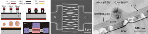
A top-down Si nanowire platform is developed to make dense array of gate-all-around (GAA) Si nanowire MOSFETs with scalable nanowire cross-section down to 4 nm on a SOI substrate. High level of local uniaxial stress (both tensile and compressive) can be integrated to this Si nanowire platform using e.g. metal gate strain and local oxidation to boost the carrier mobility. Nanowire pattern transfer to the wafer in the presence of hard mask, Si nanowire side-wall engineering by anisotropic dry Si etching (HBr/O2) to shrink further the cross-section, stress-limited oxidation and ALD high-k/metal gate stack are the key process steps.
A high level of uniaxial tensile stress (up to 5.6 GPa) is estimated in the buckled GAA Si nanowires based on a Gaussian buckling profile assumption, using top and tilted-view nanowire SEM pictures. Indeed, a significant stress level modulation (~1.2 to 5.6 GPa) is reported by the Si nanowire width modulation (44 to 4 nm) at a constant nanowire length (2 μm) on the same wafer. Non-transparency of the metal gate thin film and aggressively scaled Si nanowire cross-sections are the main technical challenges on the typical direct optical stress measurement methodologies, e.g. micro-Raman spectroscopy.
Stress-based low field electron mobility enhancement of 32% is reported in the buckled GAA sub-5 nm cross-sectional nanowires in comparison to bulk Si at the same doping level. We demonstrated such devices as high temperature performance MOSFETs (298-398 K). An ionized impurity scattering-based carrier mobility reduction mechanism is reported in a highly doped strong accumulation regime together with a threshold voltage drift of −.72 mV/K. The key MOSFET parameter extractions and device analysis in such 1DEG architectures are supported by extensive 3D TCAD device simulations.
