Surface Science, Volume 613, July 2013, Pages 35-39.
Lap Hong Chan, Shinji Hayazaki, Kokushi Ogawa, Junji Yuhara.
Department of Materials, Physics and Energy Engineering, Nagoya University, Furo-cho, Chikusa-ku, Nagoya 464-8603, Japan
Abstract
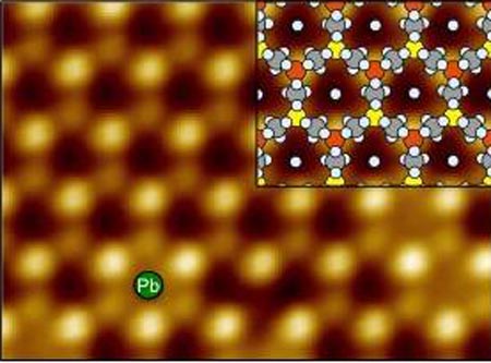
The self-organized formation of tin (Sn) and lead (Pb) atoms in a well ordered (4 × 4) vanadium oxide nanomesh on Pd(111) has been investigated using scanning tunneling microscopy (STM) and ab initiocalculations based on density functional theory (DFT). At a very low Sn coverage, most of the Sn atoms filled the vanadium oxide nanohole and a few of them were adsorbed on top of the vanadium oxide nanomesh. On the contrary, all of Pb atoms were located in the vanadium oxide nanohole. The ab initio DFT total-energy calculations indicated that the Sn and Pb atoms preferred to adsorb in the nanohole rather than on the nanomesh. The simulated STM images for the Sn and Pb atoms exhibited a local protrusion, while the experimental STM images showed a large, uniform protrusion. The adsorbed Sn and Pb atoms might be mobile in the nanohole at room temperature, possibly as a result of interaction with the STM tip.