Optics Express , Volume 21 , Issue 14 ,Page 16934. 2013.
F.S.F. Brossard, B.P.L. Reid, C.C.S. Chan, X. L. Xu, J. P. Griffiths, D.A. Williams, R. Murray, and R.A. Taylor.
Hitachi Cambridge Laboratory, Hitachi Europe Ltd., Cambridge CB3 0HE, UK and
Department of Physics, University of Oxford, Oxford OX1 3PU, UK and
Cavendish Laboratory, University of Cambridge, Cambridge, CB3 0HE, UK and
Department of Physics, Imperial College, London SW7 2AZ, UK.
Summary
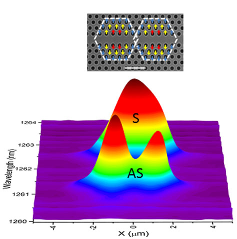
We show here that the confocal microphotoluminescence technique can give an accurate representation of the mode profile of complex photonic devices such as coupled photonic crystal cavities. The sample is kept in a fixed position whilst a laser beam scans the photonic crystal membrane containing a layer of InAs quantum dots. For more details see Appl. Phys. Lett. 88(19), 193106 (2006). The quantum dots act as point source to excite the symmetric (S) and antisymmetric (AS) resonant modes of the coupled system. Here the cavities are defined by locally shifting some holes of the photonic crystal waveguide by a few nm as indicated by the arrows. The use of a spectrometer with an InGaAs array detector enables to spectrally resolve the supermodes near telecom wavelength. We predict this technique to become invaluable as an investigation tool for future characterization of integrated nanophotonics devices.
© 2013 OSA