The International Journal of Advanced Manufacturing Technology, January 2015.
Jorge Mireles, Cesar Terrazas, Sara M. Gaytan, David A. Roberson, Ryan B. Wicker.
- W. M. Keck Center for 3D Innovation, The University of Texas at El Paso, 500 W. University Ave. Engineering Building Room 108, El Paso, TX, 79902, USA and
- Department of Mechanical Engineering, The University of Texas at El Paso, 500 W. University Ave. Engineering Building Room 108, El Paso, TX, 79902, USAand
- Department of Metallurgy and Materials Engineering, The University of Texas at El Paso, 500 W. University Ave. Engineering Building Room 108, El Paso, TX, 79902, USA
Abstract
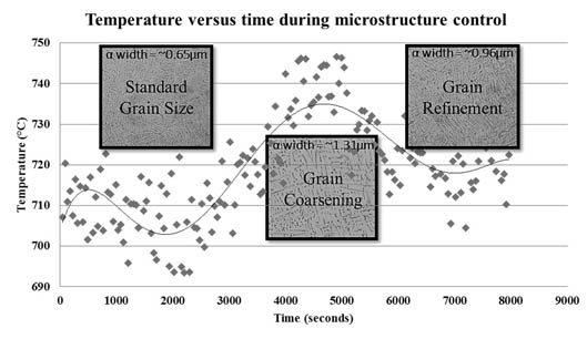
An infrared (IR) camera has been installed in an additive manufacturing Arcam A2 electron beam melting (EBM) system for improved layer-by-layer monitoring and feedback control of the EBM build process. Previous research demonstrated that temperature variations present during an EBM build (e.g., part/powder bed temperature elevates as build height increases) produce microstructural differences leading to variations in mechanical properties. Currently, the EBM system allows for process parameter modification (beam current, beam speed, beam focus, heating time) during fabrication. Modification of processing parameters can help achieve full spatial and temporal control of temperature that could lead to controlled microstructural architectures in EBM-fabricated parts. Furthermore, an automatic feedback control loop can help produce desired mechanical properties with limited user intervention. In this research, an automatic feedback control system was developed to acquire data used to create a temperature matrix of the part/powder bed surface, record information from each layer, and use the recorded information as an input to a software interface. Upon analysis of input data, the software interface communicated with Arcam’s EBM interface to change necessary parameters automatically on-demand. Results show successful manipulation of grain size in Ti-6Al-4V microstructure that ultimately can lead to three-dimensional control of microstructural architectures.
Go To The International Journal of Advanced Manufacturing Technology
Additional Information
With over 23,000 students of whom almost 80% are of Hispanic descent, UTEP is on its path towards becoming the first national research university with a 21st century student demographic. UTEP is home to a state-of-the-art additive manufacturing (AM) research center, the W.M. Keck Center for 3D Innovation (Keck Center). The Keck Center occupies 13,000 square feet of research space housing over 40 AM machines and combined facilities for AM; CAD and design; CNC machining and tooling; reverse engineering and metrology; materials characterization; mechanical testing; electronics (PCB and silicon); electromagnetics (photonics) modeling and testing; synthetic and analytical chemistry; and cell culture. Research at the Keck Center focuses on AM technology development (9 issued patents), engineered and structured materials (polymers, metals, ceramics, composites, and electronics), and advanced AM applications (aerospace, defense, energy, biomedical, and others). Research at Keck Center is made possible by its more than 50 students, faculty, and staff. In addition, the Center draws local and international interest hosting ~10,000 annual visitors ranging from multi-disciplinary professionals, K-12 students and educators, government officials, and industry leaders.