Optics Express, Vol. 21, Issue 11, pp. 13547-13554 (2013).
Chris Edwards, Kaiyuan Wang, Renjie Zhou, Basanta Bhaduri, Gabriel Popescu, and Lynford L. Goddard.
Micro and Nanotechnology Laboratory, Department of Electrical and Computer Engineering University of Illinois at Urbana-Champaign, Urbana, Illinois 61801, USA and
Quantitative Light Imaging Laboratory, Department of Electrical and Computer Engineering, Beckman Institute for Advanced Science and Technology, University of Illinois at Urbana-Champaign, Urbana, Illinois 61801, USA
Abstract
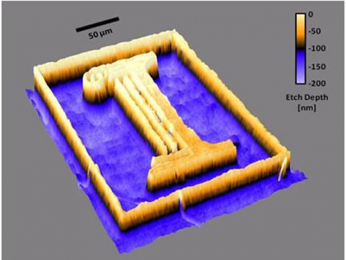
We demonstrate a maskless photochemical etching method that is capable of performing one-step etching of multi-level structures. This method uses a digital projector to focus an image onto the sample and define the etching pattern. By combining digital projection photochemical etching with diffraction phase microscopy, etch heights can be measured in situ in a non-destructive manner. This method is single shot, eliminating the need for expensive gray-scale masks or laser scanning methods. The etch rate is studied as a function of the wavelength and irradiance of the projected light. A lateral etch resolution of 2 um is demonstrated by etching selected portions of the USAF-1951 target. Micropillars, multi-level plateaus, and an Archimedean spiral are etched, each in a single processing step, to illustrate the unique capabilities.
© 2013 OSA
Additional Information
The Photonics Systems Laboratory (PSL) and Quantitative Light Imaging Laboratory (QLI) at the University of Illinois at Urbana-Champaign have worked together to develop a new technique called digital projection photochemical etching. When light with sufficient energy is absorbed near the surface of a semiconductor material, minority carriers are generated that can then diffuse to the surface and act as a catalyst in the etching process. This technique uses a standard classroom projector to focus a gray-scale image onto the sample’s surface where the projected pattern is used to define the etching. This completely alleviates the need for spin coating photoresist, aligning, exposing, and developing like in conventional photolithography. Digital projection photochemical etching can precisely etch gray-scale structures that are difficult and costly to fabricate using standard photolithography. It can also be used to etch multi-level structures in a single processing step. The wavelength (or color) of the projected light as well as the intensity of the projected pattern are adjusted in order to control etch rates and provide both spatial and material selectivity. The projected pattern may also be adjusted dynamically during the etching process. This technique is currently being used to fabricate various gray-scale structures including microlens arrays and diffractive optical elements. Furthermore, integrating the photochemical etching system into the existing epi-illumination diffraction phase microscope (epi-DPM), allows for the characterization of etched structures on site in a completely non-invasive manner (see figure below). This is not possible with scanning electron microscopy (SEM), transmission electron microscopy (TEM), atomic force microscopy (AFM), or other similar inspection methods. To learn more about the groups’ work visit: http://psl.mntl.illinois.edu and http://light.ece.illinois.edu.
Related links:
http://www.nature.com/lsa/journal/v1/n9/full/lsa201230a.html
http://www.nsf.gov/news/news_summ.jsp?cntn_id=125597
http://www.youtube.com/watch?v=6tIJqNrV20s
Figure: Watching semiconductors as they etch: epi-DPM allows us, for the first time, to watch semiconductors as they etch, tracking the instantaneous etch depths and etch rates at each pixel throughout the entire process. This new development provides the technology required to create a new multi-user cleanroom tool for wet etching that will allow the user to observe all of this information during etching, make on-the-fly adjustments to the recipe, and have full control over the process. This will greatly reduce the number of iterations required in optimizing a recipe and naturally improve the overall yield. Image courtesy of graduate student Christopher Edwards.