Significance statement
Collaborative research team lead by engineers from University of Wisconsin-Madison manage to successfully grow graphene nanoribbons with desirable semiconducting properties directly on germanium. This new technology promise to increase the performance of next-generation electronic devices
Journal Reference
Nature Communications 6, Article number:8006, 2015.
Jacobberger RM1, Kiraly B2, Fortin-Deschenes M3, Levesque PL4, McElhinny KM1, Brady GJ1, Rojas Delgado R1, Singha Roy S1, Mannix A2, Lagally MG1, Evans PG1, Desjardins P3, Martel R4, Hersam MC5, Guisinger NP6, Arnold MS1.
[expand title=”Show Affiliations”]1Department of Materials Science and Engineering, University of Wisconsin-Madison, Madison, Wisconsin 53706, USA.
21] Center for Nanoscale Materials, Argonne National Laboratory, Argonne, Illinois 60439, USA [2] Department of Materials Science and Engineering, Northwestern University, Evanston, Illinois 60208, USA.
3Department of Engineering Physics, École Polytechnique de Montréal, Montréal, Québec, Canada H3C 2A7.
4Department of Chemistry, Université de Montréal, Montréal, Québec, Canada H3C 3JT.
51] Department of Materials Science and Engineering, Northwestern University, Evanston, Illinois 60208, USA [2] Department of Chemistry, Northwestern University, Evanston, Illinois 60208, USA.
6Center for Nanoscale Materials, Argonne National Laboratory, Argonne, Illinois 60439, USA.
[/expand]
Abstract
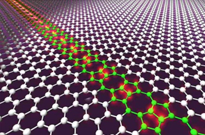
Graphene can be transformed from a semimetal into a semiconductor if it is confined into nanoribbons narrower than 10 nm with controlled crystallographic orientation and well-defined armchair edges. However, the scalable synthesis of nanoribbons with this precision directly on insulating or semiconducting substrates has not been possible. Here we demonstrate the synthesis of graphene nanoribbons on Ge(001) via chemical vapour deposition. The nanoribbons are self-aligning 3° from the Ge 110
110 directions, are self-defining with predominantly smooth armchair edges, and have tunable width to <10 nm and aspect ratio to >70. In order to realize highly anisotropic ribbons, it is critical to operate in a regime in which the growth rate in the width direction is especially slow, <5 nm h−1. This directional and anisotropic growth enables nanoribbon fabrication directly on conventional semiconductor wafer platforms and, therefore, promises to allow the integration of nanoribbons into future hybrid integrated circuits.