Microelectronics Journal, Volume 44, Issue 8, 2013, Pages 649-657.
Manas Kumar Hati, Tarun Kanti Bhattacharyya.
Advanced Technology Development Centre, IIT, Kharagpur 721302, India and
Advanced VLSI Design Laboratory, IIT, Kharagpur 721302, India and
Department of E&ECE, IIT, Kharagpur 721302, India.
Abstract
The charge pump (CP) circuit is one of the main building block in a phase-locked loop (PLL) based frequency synthesizers. In conventional CMOS charge pump circuits, there are some non-ideal effects such as clock feed through, current mismatch and charge sharing which result in a phase offset in phase-locked loop circuits.
This paper presents a new charge pump circuit in CMOS technology, which greatly reduces the mismatch of current between two branches of the cascode current mirror. By using this proposed architecture, the mismatching between the UP/DN current of the CP can be achieved with less than 0.065% from post-layout simulation. As a result the spur and also the overall phase noise of the PLL are reduced. The charge pump output voltage range is 0.40–1.25 V. Additionally, the proposed circuit has wide output voltage swing and high output resistance, which ensures its good performance under very low power supply. Further, this CP circuit is incorporated with a new switching circuit to eliminate the clock feed through and charge injection error.
Additional Information:
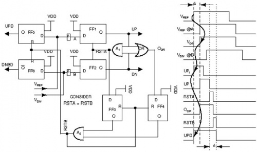
The concept of designing a switching circuit for the Charge Pump circuit in PLL has been significantly introduced in our proposed design. This technique is new and can improve the influence of clock overlapping in the UPB and UPD pulses (see Fig. 9). In conventional case when charge pump source current branch (IUP) transistor M2 is ON at that moment if there is any clock overlapping between the gate pulses of M2 and M15 (conventional case) which might introduce an extra mismatch rather than elimination of charge sharing effect. Therefore, our innovation towards this technique can help to reduce the effect of clock edge overlapping problem with the help of a very precisely controlled delay margin. Thus delay can be adjusted according to the PLL speed of operation and also basis of the design specification. However, in Ref. [6] different types of PFD have been discussed and similarly this switching concept can be implemented to all PFDs.
Future Work:
We are focusing on few things to extend our work in near future in the area of charge pump based PLL design as follows:
• Reduction of circuit area and power by removing the unity gain OTA (see Fig. 9)
• For wide range application, we are implementing loop band width controlling circuit using this concept in fractional-N PLL circuit.
• New innovative for non-overlapping clock generation circuit is still a place where we are focusing to reduce the circuit complexity and robust design technique will be introduced in terms of further phase noise improvement perspective.
• However, underlying theory behind this design is still need to be included in future.