Microelectronic Engineering, Volume 110, 2013, Pages 44-51.
Xiaolin Wang, Alla Albrecht, Hanh H. Mai, Carsten Woidt, Tamara Meinl, Michael Hornung, Martin Bartels, Hartmut Hillmer.
Institute of Nanostructure Technologies and Analytics (INA), University of Kassel, Heinrich-Plett-Str. 40, 34132 Kassel, Germany and
Center for Interdisciplinary Nanostructure Science and Technology (CINSaT), Heinrich-Plett-Str. 40, 34132 Kassel, Germany and
NanoImprint Konsortium Hessen (NIH), Heinrich-Plett-Str. 40, 34132 Kassel, Germany and
SUSS MicroTec AG, Schleissheimer Str. 90, 85748 Garching, Germany.
Abstract
We report a novel 3D NanoImprint methodology with very high vertical resolution well below 1 nm and a minimum surface roughness down to 0.2 nm in root mean square (rms) which is attractive for several applications. We introduce our 3D NanoImprint methodology in fabricating 3D filter cavities of Fabry–Pérot filter arrays for optical nanospectrometers. A large number of different cavity heights can be fabricated in one single imprint step using this high resolution, low-cost 3D NanoImprint technology. The key issue of developing 3D NanoImprint technology is the fabrication of high resolution templates. The novel 3D templates contain arrays of negative or positive checkerboard-like mesa structures with currently up to 64 different heights. Different types of 3D templates were developed and adapted to cutting edge NanoImprint methods and imprint resists. The performance of different 3D NanoImprint recipes was investigated. Based on the novel 3D NanoImprint technology developed in this work, static Fabry–Pérot filter arrays with NanoImprinted cavities indicated rather high filter transmission (best single filter >90%), small line widths (about 2 nm in full width at half maximum) and broad stop bands.
Additional Information
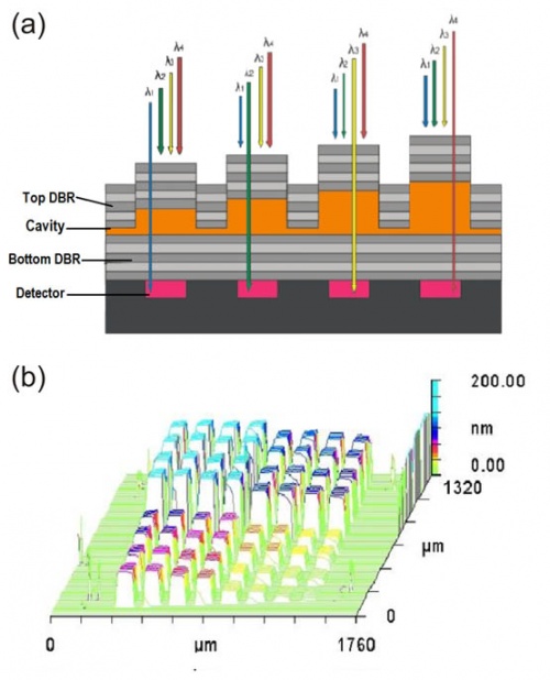
We report a novel optical spectrometer based on Fabry–Pérot filter arrays. The filter arrays comprise two identical dielectric distributed Bragg reflectors (DBRs) and transparent filter cavities with different heights whereby each cavity height determines the wavelength of the narrow transmission line of each single filter. The filter arrays will further be implemented on an array of detectors to determine the corresponding transmitted wavelengths. Since a large number of filter cavities based on different individual heights can be fabricated in a single step using NanoImprint methodology, the optical spectrometer is introduced as “nanospectrometer”.
To fabricate static filter cavities with different heights, we propose a UV-based 3D NanoImprint methodolody with the advantages of very high vertical resolution well below 1 nm and a minimum surface roughness down to 0.2 nm in root mean square (rms) which is very attractive for several applications. The key challenge in implementing the proposed 3D NanoImprint methodology is the fabrication of high vertical resolution 3D templates. The 3D templates are required to contain an array of 3D negative or positive mesa structures with the precise control of different heights. The fabrication of arbitrary different vertical heights on a template requires a number of lithography and etching steps. Using the method of digital etching, the number of fabrication runs can be reduced if the cavity heights are distributed in a digital way. Based on the method of digital etching, the fabrication of 3D template comprising maximum 64 different heights with a common step difference was demonstrated in this work.
Different types of templates were fabricated and implemented for the cutting edge NanoImprint methods such as UV-NIL and UV substrate conformal imprint lithography (UV-SCIL). The NanoImprint recipe characterized by different resist materials and process parameters was investigated. The novel 3D NanoImprint technology was developed and implemented in this work and the Fabry–Pérot filter arrays with NanoImprinted cavities indicated rather high filter transmission (best single filter >90%), small line widths (about 2 nm in full width at half maximum) and broad stop bands.
Figure Legend
(a) Design schematic of a Fabry–Pérot-filter-array-based nanospectrometer (left) and its corresponding transmission spectra (right); (b) White light interferometry (WLI) measurement: topography of 3D templates containing arrays of ‘‘positive’’ mesa structures of 64 different heights.