Small, Volume 9, Issue 23, page 4088, December 9, 2013.
Dai Zhang2, Alfred J. Meixner2, Frank Schreiber1,Dieter P. Kern1 , Monika Fleischer1,*
1. Institute for Applied Physics and Center LISA[+], Eberhard Karls Universität Tübingen, Auf der Morgenstelle 10, 72076 Tübingen, Germany.
2. Institute of Physical and Theoretical Chemistry and Center LISA[+], Eberhard Karls Universität Tübingen, Auf der Morgenstelle 15, 72076 Tübingen, Germany.
Abstract
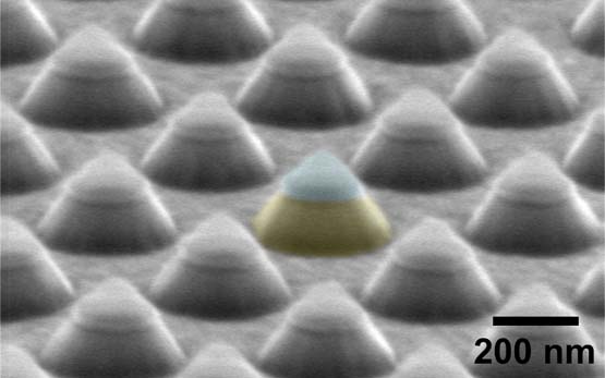
Ordered arrays of nanocones and nanopyramids are fabricated in a fully parallel approach by M. Fleischer and co-workers, as reported on page 3987. Single or double layers of self-assembled nanospheres are directly modified or used as templates for the creation of etch masks. Nanocones with sharp tips form when the masks are transferred into a gold or silver layer. Under optical excitation, narrowly confi ned hotspots are created near the cone tips. These structures have interesting properties for nano-optical applications and are evaluated as substrates for surface enhanced Raman spectroscopy using a thin film of pentacene molecules.
Copyright © 2013 WILEY-VCH Verlag GmbH & Co. KGaA, Weinheim.
Figure Legend
“Fabrication of an array of gold nanocones for surface enhanced Raman scattering. Intermediate scanning electron microscope image of truncated gold nanocones with caps after ion milling a gold film with polystyrene spheres on top for some time.”