Journal of Alloys and Compounds, Volume 554, 25 March 2013, Pages 246-253.
Artur Trembulowicz, Leszek Jurczyszyn, Zbigniew Szczudlo, Antoni Ciszewski
Institute of Experimental Physics, University of Wroclaw, plac Maxa Borna 9, 50-204 Wroclaw, Poland
Abstract
Surface alloying in the Hf/W(1 0 0) adsorption system was studied using STM, LEED and AES. Vapor-deposited, Hf layers of average thickness from 0.2 to 2 geometrical monolayers were gradually annealed at various temperatures from 300 to 2100 K. Formation of two ordered c(2 × 4) and R26.6 phases was observed above 1200 K. Both phases had a domain morphology and were observed up to 2100 K. Theab initio structural calculations indicate that the phases correspond to Hf3W and Hf4W ordered surface alloys, respectively.
Additional Information:
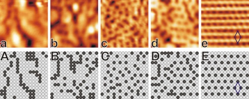
It is well known that Hf and W form the Laves phase HfW2 of atomic compactness higher than those of the close packed fcc and hcp metals [1]. The phase has promising mechanical properties at high temperatures [3]. The aim of the studies presented here was to investigate surface alloy formation at a bimetallic surface made by Hf deposition onto the surface of W(100). Thermodynamically controlled topographical and structural changes caused by annealing have been studied by scanning tunneling microscopy (STM) supported the ab initio structural calculations, and by low energy electron diffraction (LEED) and Auger electron spectroscopy (AES) complementarily. It has been found out that two surface alloys Hf3W and Hf4W are formed at this system depending on the amount of Hf deposited. The alloys decay above 2000 K. Enclosed figure demonstrate an example series of sequential steps of Hf3W surface alloy nucleation during annealing at temperature about 1400K (STM topographies (a) – (d), and corresponding ball models (A) – (D)). The STM topography (e) and the ball model (E) depict fully developed 2D alloy after annealing at about 2000 K. Grains of the 2D Hf3W alloy grows with the annealing temperature increase. An average diameter of well-developed grains after annealing at 2000 K exceeds the imaging area of the STM topographies (5 x 5 nm2) shown in the figure. The grains are epitaxially oriented against the substrate producing, in the case of the Hf3W surface alloy, c(2×4) or c(4×2) domains.
[1] A. Massalski (Ed.), Binary Alloy Phase Diagrams, vol. 2, American Society for Metals, Metals Park, OH, 1986, p. 3495. [2] W.D. Cai, Y. Li, R.J. Dowding, F.A. Mohamed, E.J. Lavernia, Rev. Part. Mater. 3(1995) 71. [3] E. Lassner, W.D. Schubert, Tungsten: Properties, Chemistry, Technology of the Element, Alloys, and Chemical Compounds, Springer, Verlag, 1999, pp. 255–305.
Figure caption:
(a) – (d) A series of STM topographies showing sequential steps of Hf3W surface alloy nucleation during annealing at ~ 1400 K. (e) STM topography of a well-developed 2D grain of the alloy after annealing at ~ 2000 K. (A) – (E) corresponding ball models. Elementary unit cell of the Hf3W alloy is marked in (e) and (E). Areas where the alloy is formed are atomically resolved. Imaged area: 5 x 5 nm2.