
Significance Statement
Plasma approaches that are applied to nanocarbon materials and devices are expected to be extensively developed for the purpose of solving a range of underlying global issues related to energy/environment, electronics/mechanics, bio/food technologies, medical treatment, and so on. Here plasma processing techniques, which allow versatile control of both chemical and physical aspects, have been demonstrated to enable the innovative synthesis and functionalization of three varieties of low-dimensional nanocarbons, contributing to the development of such prospective applications.
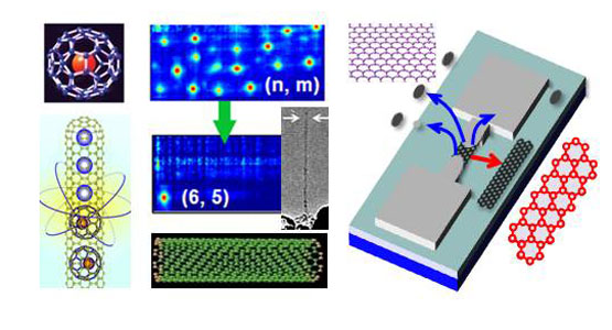
One goal is the high-yield production of atom encapsulated (@) fullerenes, where the control of alkali-fullerene plasma leads to the macro-quantity formation of charge-exploited Li@C60 for the first time. Also, the highest purity of 〜1 %, almost two orders of magnitude higher than that obtained by other methods, of spin-exploited N@C60 is realized by the control of electron-beam and impinging-ion energies in the double plasma device. Following 0-D fullerenes, in the case of 1-D carbon nanotubes the challenge is precise structure control, i.e., chirality control of single-walled carbon nanotubes (SWNTs), which is crucial for electronics applications. The extremely narrow-chirality distributed growth of SWNTs is realized with time-programmed and nonmagnetic-catalyzed plasma CVD. As for functionalization of SWNTs, the enhanced p-type C60@SWNTs forming heterojunctions with n-type Si and pn-junction-embedded SWNTs created under the substrate-bias control in collisionless plasmas are found to be effective for harvesting solar energy in the infrared wavelength range. Moreover, the energy conversion efficiency is observed to suddenly increase for light energies higher than two times the band gap, suggesting the occurrence of multiple exciton generation in the C60@SWNT-based solar cell. The third target is structure-controlled functional 2-D graphene, where several issues for practical applications have to be overcome. The direct growth of centimeter-order, uniform, and high-quality single-layer graphene on an insulating SiO2 substrate is realized by using low-temperature diffusion plasma CVD. The doping density of directly grown graphene on the SiO2 substrate is controlled by adding carrier-resources gas such as NH3 during plasma CVD. Furthermore, to induce semiconducting properties in graphene, which has metallic properties, a novel method for graphene nanoribbon growth with precise site and alignment control, which is simple and scalable, is established using Ni nanobars and Rapid Heating Plasma CVD (RH-PCVD). Here, the graphene nanoribbon FET directly made by RH-PCVD shows a high on/off ratio (>104) with a clear transport gap (≈ 58.5 meV).
Journal Reference
Plasma Chemistry and Plasma Processing, 2014, Volume 34, Issue 3, pp 377-402. Rikizo Hatakeyama, Toshiaki Kato, Yongfeng Li, Toshiro Kaneko.
Department of Electronic Engineering, Tohoku University, 6-6-05 Aoba, Aramaki, Aoba-ku, Sendai, 980-8579, Japan and
State Key Laboratory of Heavy Oil Processing, China University of Petroleum, Beijing Changping, 102249, China.
Abstract
Our recent research has shown that plasma processing techniques, which allow versatile control of both chemical and physical aspects, have considerable potential for the innovative synthesis and functionalization of three varieties of low-dimensional nanocarbons, which show great promise in the development of nanoscience and its applications. In the case of 0-D fullerenes, the mission is the high-yield production of atom (X) encapsulated fullerenes (X@C60). The formation of macro-quantities of charge-exploited Li@C60 and overwhelmingly-high purity spin-exploited N@C60 are realized for the first time by the control of alkali-fullerene and nitrogen double plasmas, respectively. In the case of 1-D carbon nanotubes the challenge is precise structure control, i.e., chirality control of single-walled carbon nanotubes (SWNTs). The extremely narrow-chirality distributed growth of SWNTs is realized with time-programmed and nonmagnetic-catalyzed plasma CVD. As for functionalization of SWNTs, the enhanced p-type C60@SWNTs created under the substrate-bias control in collisionless plasmas are found to be effective for harvesting solar energy in the infrared wavelength range and adapted to the use for multiple exciton generation in solar cells. Concerning 2-D graphene, our aim is to overcome two serious issues for electronics applications. One is the realization of the direct growth of graphene on an insulating (SiO2) substrate by adjusting the growth parameters using non-equilibrium diffusion plasma CVD. The other is the direct fabrication of field-effect transistor device of a narrow-width (≥20 nm) graphene nanoribbon using a new, simple, and scalable method based on rapid heating plasma CVD, which shows a clear transport gap and a high on/off ratio. Finally the prospects for the above-mentioned results are discussed together with ripple effects of the nanocarbon research on the progress of nanoscience and its applications.
Go To Plasma Chemistry and Plasma Processing
