Applied Physics A, 2013, Volume 112, Issue 3, pp 517-523.
Zhiya Dang, Agnieszka Banas, Sara Azimi, Jiao Song, Mark Breese, Yong Yao, Shuvan Prashant Turaga, Gonzalo Recio-Sánchez, Andrew Bettiol, Jeroen Van Kan.
Centre for Ion Beam Applications (CIBA), Department of Physics, National University of Singapore, Singapore, 117542, Singapore and
Singapore Synchrotron Light Source (SSLS), National University of Singapore, 5 Research Link, Singapore, 117603, Singapore and
Departamento de Física Aplicada, Universidad Autónoma de Madrid, 28049, Cantoblanco, Madrid, Spain.
Abstract
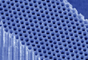
A 3D silicon micromachining method based on proton beam writing combined with electrochemical anodization of p-type silicon enables fabrication of mid-infrared photonic crystals made of silicon and porous silicon. Here, example structures of silicon 1D and 2D photonic crystals are demonstrated. Progress and problems of fabricating 3D photonic crystals made of silicon are discussed. The strategy of fabricating photonic crystals purely made of porous silicon, and the characterization method of all these mid-infrared structures, are discussed. Due to the flexibility of this fabrication method, photonic devices and integrated photonic circuits may be built on a single chip, for which two 2D silicon photonic crystals with one on top of the other are demonstrated.