Significant statement
Prof. Maki Suemitsu’s group at Tohoku University in Japan, in collaboration with a group at Sumitomo Electric Industries. Ltd, reports a substantial betterment of the epitaxial graphene (EG) on Si substrates by adding an AlN thin interlayer in between 3C-SiC thin film and the Si substrate. In this new Gr/SiC/AlN/Si heterostructure, the large (~20%) lattice mismatch between Si and SiC crystals is now born at the AlN/Si interface, which somehow greatly improves the quality of the 3C-SiC thin film and of EG thereon. The AlN interlayer also contributes to suppression of the Si out-diffusion from the Si substrate during the high-temperature graphitization, which allows use of chemo-mechanical polishing (CMP) before graphitization. Since graphene is known to be a promising candidate for the next-generation high mobility material, this development opens up a way to future THz devices.
Journal of Physics D: Applied Physics Volume 47 Number 9,2014.
Maki Suemitsu1, Sai Jiao1, Hirokazu Fukidome1, Yasunori Tateno2, Isao Makabe2 and Takashi Nakabayashi2
1 Research Institute of Electrical Communications, Tohoku University, Sendai 980–8577, Japan and
2 Transmisson Devices R&D Laboratories, Sumitomo Electric Industries. Ltd, Yokohama, 224–0845,Japan
Abstract
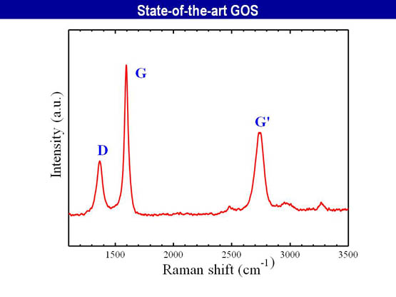
By forming a thin 3C-SiC film on Si substrates and by annealing it at ~1500 K in vacuo, few-layer graphene is formed epitaxially on Si substrates. In this graphene-on-silicon (GOS) technology, graphene grows at least on three major low-index Si surfaces: (1 1 1), (1 0 0) and (1 1 0), which allows tuning of structural and electronic properties of epitaxial graphene by simply controlling the crystallographic orientation of the surface. A typical example can be found in the two types of graphene formed on 3C-SiC(1 1 1) surfaces; the one on 3C-SiC(1 1 1)/Si(1 1 1) shows a Bernal stacking with an interfacial buffer layer, while the one on 3C-SiC(1 1 1)/Si(1 1 0) shows a non-Bernal stacking without an interfacial buffer layer. Inserting an AlN interlayer between Si and 3C-SiC significantly contributes to improvement of the GOS quality. Moreover, thanks to the sealing effect of the AlN layer against Si out-diffusion, we can apply chemomechanical polishing of SiC surface to reduce the surface roughness, which can further accentuate the effect of H2 annealing of the surface. As a result, a D to G band intensity ratio as low as 0.4 is obtained.